Hardwired Programmable Control Unit Design Example (Single Cycle Computer)
The following is a design for a simple 16-bit computer which can be seen as an example design of a hardwired programmable control unit.
A programmable control unit executes instructions which configure the datapath to perform certain operations, for example, adding the contents of two registers, writing a value to a memory location, etc. Because the instructions will need to be determined before the design of the control unit can be completed, we list these instructions now. For each instruction the following is given:
- a description of the instruction in English,
- a 16-bits wide bit pattern which identifies the instruction,
- a description of the instruction in the form of a RTL expression, and
- a list of processor flags (status bits) that are updated.
The symbols used are as follows:
- ⇐ - a register transfer.
- & - the logical and (conjunction) operator.
- | - the logical or (disjunction) operator.
- ^ - the logical exclusive-or operator.
- ~ - the logical negation/complement operator.
- == - the equality operator.
- C - the Carry flag.
- if - the conditional operator.
- INPUT - the contents of the input port.
- MEMORY[L] - the contents of the memory at location L.
- N - the Negative flag.
- OUTPUT - the contents of the output port.
- PC - the Program Counter.
- rA - the register with address A.
- S - a bit of a signed value.
- sext(V) - the value V is sign extended to 16-bits. Example: sext(101) = 1111111111111101.
- U - a bit of an unsigned value.
- V - the oVerflow flag.
- X - a bit value which can be either 1 or 0.
- Z - the Zero flag.
- zerofill(V) - the value V is extended to 16-bits with zeroes. Example: zerofill(101) = 0000000000000101.
And here are the instructions:
ADD
This instruction adds the contents of two registers and stores the result in a third.
| 15 | 14 | 13 | 12 | 11 | 10 | 9 | 8 | 7 | 6 | 5 | 4 | 3 | 2 | 1 | 0 |
|---|---|---|---|---|---|---|---|---|---|---|---|---|---|---|---|
| 0 | 0 | 1 | 0 | 0 | 0 | 0 | D | D | D | B | B | B | A | A | A |
rD ⇐ rA + rB
Flags: C, N, V, and Z.
ADDI
This instruction adds the contents of a register with an 3-bit unsigned integer and stores the result in another register.
| 15 | 14 | 13 | 12 | 11 | 10 | 9 | 8 | 7 | 6 | 5 | 4 | 3 | 2 | 1 | 0 |
|---|---|---|---|---|---|---|---|---|---|---|---|---|---|---|---|
| 1 | 1 | 0 | 0 | 0 | 0 | 0 | D | D | D | U | U | U | A | A | A |
rD ⇐ rA + zerofill(UUU)
Flags: C, N, V, and Z.
AND
This instruction performs the logical and (conjunction) of the contents of two registers and stores the result in a third.
| 15 | 14 | 13 | 12 | 11 | 10 | 9 | 8 | 7 | 6 | 5 | 4 | 3 | 2 | 1 | 0 |
|---|---|---|---|---|---|---|---|---|---|---|---|---|---|---|---|
| 0 | 0 | 1 | 0 | 0 | 1 | 0 | D | D | D | B | B | B | A | A | A |
rD ⇐ rA & rB
Flags: Z.
BCC
If the C flag is clear then this instruction branches to the address given by the current contents of the PC register plus the given offset.
| 15 | 14 | 13 | 12 | 11 | 10 | 9 | 8 | 7 | 6 | 5 | 4 | 3 | 2 | 1 | 0 |
|---|---|---|---|---|---|---|---|---|---|---|---|---|---|---|---|
| 1 | 0 | 1 | 0 | 1 | 0 | 0 | S | S | S | S | S | S | S | S | S |
if C==0 then PC ⇐ PC + sext(SSSSSSSSS)
Flags: None.
BCS
If the C flag is set then this instruction branches to the address given by the current contents of the PC register plus the given offset.
| 15 | 14 | 13 | 12 | 11 | 10 | 9 | 8 | 7 | 6 | 5 | 4 | 3 | 2 | 1 | 0 |
|---|---|---|---|---|---|---|---|---|---|---|---|---|---|---|---|
| 1 | 0 | 1 | 0 | 0 | 0 | 0 | S | S | S | S | S | S | S | S | S |
if C==1 then PC ⇐ PC + sext(SSSSSSSSS)
Flags: None.
BNC
If the N flag is clear then this instruction branches to the address given by the current contents of the PC register plus the given offset.
| 15 | 14 | 13 | 12 | 11 | 10 | 9 | 8 | 7 | 6 | 5 | 4 | 3 | 2 | 1 | 0 |
|---|---|---|---|---|---|---|---|---|---|---|---|---|---|---|---|
| 1 | 0 | 1 | 0 | 1 | 0 | 1 | S | S | S | S | S | S | S | S | S |
if N==0 then PC ⇐ PC + sext(SSSSSSSSS)
Flags: None.
BNS
If the N flag is set then this instruction branches to the address given by the current contents of the PC register plus the given offset.
| 15 | 14 | 13 | 12 | 11 | 10 | 9 | 8 | 7 | 6 | 5 | 4 | 3 | 2 | 1 | 0 |
|---|---|---|---|---|---|---|---|---|---|---|---|---|---|---|---|
| 1 | 0 | 1 | 0 | 0 | 0 | 1 | S | S | S | S | S | S | S | S | S |
if N==1 then PC ⇐ PC + sext(SSSSSSSSS)
Flags: None.
BVC
If the V flag is clear then this instruction branches to the address given by the current contents of the PC register plus the given offset.
| 15 | 14 | 13 | 12 | 11 | 10 | 9 | 8 | 7 | 6 | 5 | 4 | 3 | 2 | 1 | 0 |
|---|---|---|---|---|---|---|---|---|---|---|---|---|---|---|---|
| 1 | 0 | 1 | 0 | 1 | 1 | 0 | S | S | S | S | S | S | S | S | S |
if V==0 then PC ⇐ PC + sext(SSSSSSSSS)
Flags: None.
BVS
If the V flag is set then this instruction branches to the address given by the current contents of the PC register plus the given offset.
| 15 | 14 | 13 | 12 | 11 | 10 | 9 | 8 | 7 | 6 | 5 | 4 | 3 | 2 | 1 | 0 |
|---|---|---|---|---|---|---|---|---|---|---|---|---|---|---|---|
| 1 | 0 | 1 | 0 | 0 | 1 | 0 | S | S | S | S | S | S | S | S | S |
if V==1 then PC ⇐ PC + sext(SSSSSSSSS)
Flags: None.
BZC
If the Z flag is clear then this instruction branches to the address given by the current contents of the PC register plus the given offset.
| 15 | 14 | 13 | 12 | 11 | 10 | 9 | 8 | 7 | 6 | 5 | 4 | 3 | 2 | 1 | 0 |
|---|---|---|---|---|---|---|---|---|---|---|---|---|---|---|---|
| 1 | 0 | 1 | 0 | 1 | 1 | 1 | S | S | S | S | S | S | S | S | S |
if Z==0 then PC ⇐ PC + sext(SSSSSSSSS)
Flags: None.
BZS
If the Z flag is set then this instruction branches to the address given by the current contents of the PC register plus the given offset.
| 15 | 14 | 13 | 12 | 11 | 10 | 9 | 8 | 7 | 6 | 5 | 4 | 3 | 2 | 1 | 0 |
|---|---|---|---|---|---|---|---|---|---|---|---|---|---|---|---|
| 1 | 0 | 1 | 0 | 0 | 1 | 1 | S | S | S | S | S | S | S | S | S |
if Z==1 then PC ⇐ PC + sext(SSSSSSSSS)
Flags: None.
IN
This instruction moves the contents of the input port to a register.
| 15 | 14 | 13 | 12 | 11 | 10 | 9 | 8 | 7 | 6 | 5 | 4 | 3 | 2 | 1 | 0 |
|---|---|---|---|---|---|---|---|---|---|---|---|---|---|---|---|
| 1 | 1 | 1 | 0 | 0 | 0 | 0 | D | D | D | X | X | X | X | X | X |
rD ⇐ INPUT
Flags: None.
JMP
This instruction jumps to the address given by the current contents of the PC register plus the given offset.
| 15 | 14 | 13 | 12 | 11 | 10 | 9 | 8 | 7 | 6 | 5 | 4 | 3 | 2 | 1 | 0 |
|---|---|---|---|---|---|---|---|---|---|---|---|---|---|---|---|
| 1 | 0 | 0 | 0 | 0 | 0 | 0 | S | S | S | S | S | S | S | S | S |
PC ⇐ PC + sext(SSSSSSSSS)
Flags: None.
LD
This instruction loads a register with the contents of memory at the location given by the contents of another register.
| 15 | 14 | 13 | 12 | 11 | 10 | 9 | 8 | 7 | 6 | 5 | 4 | 3 | 2 | 1 | 0 |
|---|---|---|---|---|---|---|---|---|---|---|---|---|---|---|---|
| 0 | 1 | 0 | 0 | 0 | 0 | 0 | D | D | D | X | X | X | A | A | A |
rD ⇐ MEMORY[rA]
Flags: Z.
MOV
This instruction moves the contents of one register to another.
| 15 | 14 | 13 | 12 | 11 | 10 | 9 | 8 | 7 | 6 | 5 | 4 | 3 | 2 | 1 | 0 |
|---|---|---|---|---|---|---|---|---|---|---|---|---|---|---|---|
| 0 | 0 | 1 | 1 | 0 | 0 | 0 | D | D | D | X | X | X | A | A | A |
rD ⇐ rA
Flags: Z.
NOP
This instruction does nothing.
| 15 | 14 | 13 | 12 | 11 | 10 | 9 | 8 | 7 | 6 | 5 | 4 | 3 | 2 | 1 | 0 |
|---|---|---|---|---|---|---|---|---|---|---|---|---|---|---|---|
| 0 | 0 | 0 | 0 | 0 | 0 | 0 | 0 | 0 | 0 | 0 | 0 | 0 | 0 | 0 | 0 |
Flags: none.
NOT
This instruction performs the logical not (negation, complement) of the contents of one register and stores the result in another.
| 15 | 14 | 13 | 12 | 11 | 10 | 9 | 8 | 7 | 6 | 5 | 4 | 3 | 2 | 1 | 0 |
|---|---|---|---|---|---|---|---|---|---|---|---|---|---|---|---|
| 0 | 0 | 1 | 0 | 1 | 0 | 1 | D | D | D | X | X | X | A | A | A |
rD ⇐ ~rA
Flags: Z.
OR
This instruction performs the logical or (disjunction) of the contents of two registers and stores the result in a third.
| 15 | 14 | 13 | 12 | 11 | 10 | 9 | 8 | 7 | 6 | 5 | 4 | 3 | 2 | 1 | 0 |
|---|---|---|---|---|---|---|---|---|---|---|---|---|---|---|---|
| 0 | 0 | 1 | 0 | 0 | 1 | 1 | D | D | D | B | B | B | A | A | A |
rD ⇐ rA | rB
Flags: Z.
OUT
This instruction moves the contents of a register to the output port.
| 15 | 14 | 13 | 12 | 11 | 10 | 9 | 8 | 7 | 6 | 5 | 4 | 3 | 2 | 1 | 0 |
|---|---|---|---|---|---|---|---|---|---|---|---|---|---|---|---|
| 1 | 1 | 1 | 0 | 0 | 0 | 1 | X | X | X | X | X | X | A | A | A |
OUTPUT ⇐ rA
Flags: None.
SL
This instruction shifts the contents of a register one place to the left and stores this result in another register.
| 15 | 14 | 13 | 12 | 11 | 10 | 9 | 8 | 7 | 6 | 5 | 4 | 3 | 2 | 1 | 0 |
|---|---|---|---|---|---|---|---|---|---|---|---|---|---|---|---|
| 0 | 0 | 1 | 1 | 0 | 1 | 0 | D | D | D | X | X | X | A | A | A |
rD ⇐ rA << 1
Flags: Z.
SR
This instruction shifts the contents of a register one place to the right and stores this result in another register.
| 15 | 14 | 13 | 12 | 11 | 10 | 9 | 8 | 7 | 6 | 5 | 4 | 3 | 2 | 1 | 0 |
|---|---|---|---|---|---|---|---|---|---|---|---|---|---|---|---|
| 0 | 0 | 1 | 1 | 0 | 0 | 1 | D | D | D | X | X | X | A | A | A |
rD ⇐ rA >> 1
Flags: Z.
ST
This instruction stores the contents of a register into the memory at the location given by the contents of another register.
| 15 | 14 | 13 | 12 | 11 | 10 | 9 | 8 | 7 | 6 | 5 | 4 | 3 | 2 | 1 | 0 |
|---|---|---|---|---|---|---|---|---|---|---|---|---|---|---|---|
| 0 | 1 | 1 | 0 | 0 | 0 | 0 | X | X | X | B | B | B | A | A | A |
MEMORY[rA] ⇐ rB
Flags: Z.
SUB
This instruction subtracts the contents of one register from a second register and stores the result in a third.
| 15 | 14 | 13 | 12 | 11 | 10 | 9 | 8 | 7 | 6 | 5 | 4 | 3 | 2 | 1 | 0 |
|---|---|---|---|---|---|---|---|---|---|---|---|---|---|---|---|
| 0 | 0 | 1 | 0 | 0 | 0 | 1 | D | D | D | B | B | B | A | A | A |
rD ⇐ rA - rB
Flags: C, N, V, and Z.
SUBI
This instruction subtracts a 3-bit unsigned integer from the contents of a register and stores the result in another register.
| 15 | 14 | 13 | 12 | 11 | 10 | 9 | 8 | 7 | 6 | 5 | 4 | 3 | 2 | 1 | 0 |
|---|---|---|---|---|---|---|---|---|---|---|---|---|---|---|---|
| 1 | 1 | 0 | 0 | 0 | 0 | 1 | D | D | D | U | U | U | A | A | A |
rD ⇐ rA - zerofill(UUU)
Flags: C, N, V, and Z.
XOR
This instruction performs the logical xor (exclusive-or) of the contents of two registers and stores the result in a third.
| 15 | 14 | 13 | 12 | 11 | 10 | 9 | 8 | 7 | 6 | 5 | 4 | 3 | 2 | 1 | 0 |
|---|---|---|---|---|---|---|---|---|---|---|---|---|---|---|---|
| 0 | 0 | 1 | 0 | 1 | 0 | 0 | D | D | D | B | B | B | A | A | A |
rD ⇐ rA ^ rB
Flags: Z.
ZERO
This instruction stores zero in the contents of a register
| 15 | 14 | 13 | 12 | 11 | 10 | 9 | 8 | 7 | 6 | 5 | 4 | 3 | 2 | 1 | 0 |
|---|---|---|---|---|---|---|---|---|---|---|---|---|---|---|---|
| 0 | 0 | 1 | 1 | 0 | 1 | 1 | D | D | D | X | X | X | X | X | X |
rD ⇐ 0
Flags: Z.
Top-level Design
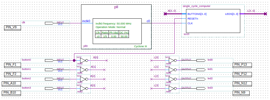
The computer will be implemented on an Altera Cyclone III FPGA Starter Kit board. We will have only basic I/O circuits: four LEDs for output, and four push buttons for input. The schematic below shows the computer, the input and output pins, and the system clock.
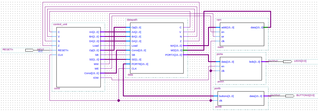
The schematic below shows the inside of the single cycle computer block. We see that it comprises a control unit, a datapath, some random access memory (RAM), and the two I/O ports.
Control Unit
The control unit comprises a program counter, a read only memory (ROM), an instruction decoder, a branch control block, a sign extension block, and a zero fill block. The following schematic shows the configuration:
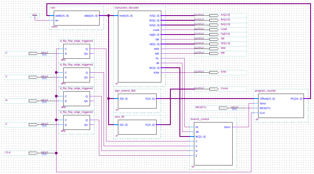
The program counter holds the address of the current instruction which is held in ROM. This 16-bit instruction is decoded into a number of control signals sent to the datapath and to the branch control block. The branch control block determines how we calculate the next program counter address: we either calculate a new address using an offset when we jump or branch, or we just increment the current address by one. The sign extension block is used to calculate the jump and branch offset from bits in the instruction. It extends a 9-bit value to a 16-bit offset. The zero fill block is used to create a 16-bit value from 3 bits of the instruction by filling in the most significant 13 bits with zero.
The code for the top-level of the control unit follows:
module control_unit(AA, BA, DA, Load, Op, SB, SD, MW, ME, Const, IOW, C, V, N, Z, RESETn, CLK);
   output [2:0] AA;      // A register Address.
   output [2:0] BA;      // B register Address.
   output [2:0] DA;      // D register Address.
   output 	Load;    // Load D register
   output [3:0] Op;      // Function unit Operation.
   output 	SB;      // Muxb selector.
   output [1:0]	SD;      // Muxd selector.
   output 	MW;      // Memory Write
   output 	ME;      // Memory Enable
   output 	IOW;    // IO port Write.
   output [15:0] Const;  // Constant (Immediate operand)
   input 	 C;      // Carry status bit.
   input 	 V;      // oVerflow status bit.
   input 	 N;      // Negative status bit.
   input 	 Z;      // Zero status bit.
   input 	 RESETn; // Reset signal (active low).
   input 	 CLK;    // System clock.

   wire [2:0] 	 BC;
   wire [15:0] 	 Instr;
   wire [15:0] 	 Offset;
   wire [15:0] 	 PC;
   wire 	 SIncr;
   wire 	 PL;
   wire 	 JB;
   wire 	 CQ, CQn;
   wire 	 NQ, NQn;
   wire 	 VQ, VQn;
   wire 	 ZQ, ZQn;

   d_flip_flop_edge_triggered dffC(CQ, CQn, CLK, C);
   d_flip_flop_edge_triggered dffN(NQ, NQn, CLK, N);
   d_flip_flop_edge_triggered dffV(VQ, VQn, CLK, V);
   d_flip_flop_edge_triggered dffQ(ZQ, ZQn, CLK, Z);

   branch_control bc(SIncr, PL, JB, BC, CQ, VQ, NQ, ZQ);
   rom mem(Instr, PC, 1'b1);
   sign_extend_9bit se(Offset, Instr[8:0]);
   zero_fill zf(Const, Instr[5:3]);
   program_counter pc(PC, Offset, SIncr, RESETn, CLK);
   instruction_decoder id(AA, BA, DA, Load, Op, SB, SD, MW, ME, PL, JB, BC, IOW, Instr);
endmodule // control_unit
ROM
The ROM is just a combinational circuit which has a small test program.
module rom (data, addr, en);
   output [15:0] data;
   input 	en;
   input [15:0] addr;

   wire [15:0] 	odata;

   assign odata = (addr == 16'h0000)   ? 16'b0011011_001_000_000     // ZERO $1
		  : (addr == 16'h0001) ? 16'b1110000_000_000_000     // IN $0
		  : (addr == 16'h0002) ? 16'b0010101_000_000_000     // NOT $0, $0
		  : (addr == 16'h0003) ? 16'b0110000_000_000_001     // ST $1, $0
		  : (addr == 16'h0004) ? 16'b0100000_010_000_001     // LD $2, $1
		  : (addr == 16'h0005) ? 16'b1110001_000_000_010     // OUT $2
		  : (addr == 16'h0006) ? 16'b1000000_111111010       // JMP 0000
		  : 16'h00;                                          // NOP

   assign data = en ? odata : 16'bz;
endmodule // rom
Program Counter
From the schematic below we see that the program counter is more than just a counter.
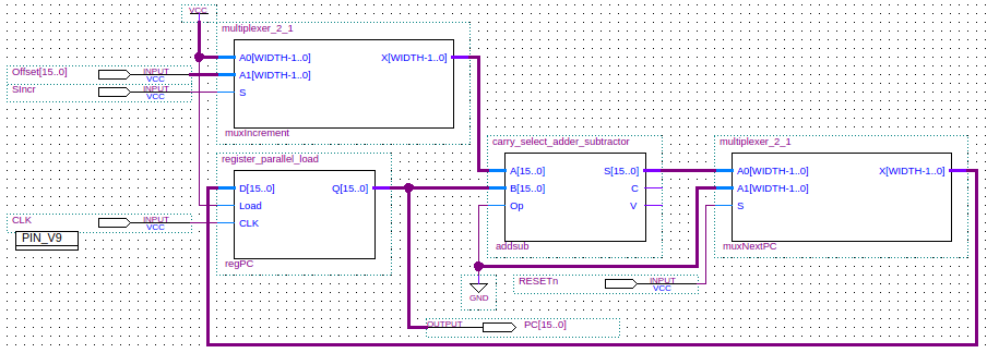
Here we see that we set the contents of the counter to zero when a reset occurs, and we increment the counter on each clock cycle, either by one if this is not a jump or a branch, or by an offset otherwise.
module program_counter(PC, Offset, SIncr, RESETn, CLK);
   output [15:0] PC;
   input [15:0]  Offset;
   input 	 SIncr;
   input 	 RESETn;
   input 	 CLK;

   wire 	 IncC;   // Carry from the increment op. (ignored)
   wire 	 IncV;   // oVerflow from the increment op. (ignored)
   wire [15:0] 	 NextPC; // The next Program Counter register value.
   wire [15:0] 	 Increment;
   wire [15:0] 	 IncrementedPC;

   multiplexer_2_1 muxIncrement(Increment, 16'h0001, Offset, SIncr);
   register_parallel_load pc(PC, NextPC, 1'b1, CLK);
   carry_select_adder_subtractor addsub(IncrementedPC, IncC, IncV, PC, Increment, 1'b0);
   multiplexer_2_1 muxNextPC(NextPC, 16'h0000, IncrementedPC, RESETn);
endmodule // program_counter
Branch Control
The branch control block outputs a signal which is fed into the program counter's multiplexer which chooses the program counter increment. This output signal is set if the current instruction is a jump or if it is a branch and the condition is fulfilled.
module branch_control(SIncr, PL, JB, BC, C, V, N, Z);
   output      SIncr;
   input       PL; // Program counter Load.
   input       JB; // 0 => Branch, 1 => Jump.
   input [2:0] BC; // Branch condition.
   input       C;  // Carry.
   input       V;  // Overflow.
   input       N;  // Negative.
   input       Z;  // Zero.

   wire        Cn, Vn, Nn, Zn;
   wire        Cond;
   wire        w1;

   not(Cn, C);
   not(Vn, V);
   not(Nn, N);
   not(Zn, Z);

   multiplexer_8_1 #(1) muxa(Cond, C, V, N, Z, Cn, Vn, Nn, Zn, BC);
   or(w1, JB, Cond);
   and(SIncr, w1, PL);
endmodule // branch_control
Instruction Decoder
The job of the instruction decoder is to generate the appropriate signals to the datapath and to other parts of the control unit for each instruction. The table below shows each instruction and the decoder's output signals. Here X means an input or output can be anything ("don't care"), and A, B, D, are used to directly connect instruction bit fields to output signals.
| Instruction | DA | BA | AA | Op | SD | BC | ||||||||||||||||||||||||||||||||||
|---|---|---|---|---|---|---|---|---|---|---|---|---|---|---|---|---|---|---|---|---|---|---|---|---|---|---|---|---|---|---|---|---|---|---|---|---|---|---|---|---|
| Mnemonic | 15 | 14 | 13 | 12 | 11 | 10 | 9 | 8 | 7 | 6 | 5 | 4 | 3 | 2 | 1 | 0 | 2 | 1 | 0 | 2 | 1 | 0 | 2 | 1 | 0 | SB | 3 | 2 | 1 | 0 | 1 | 0 | Load | MW | PL | JB | 2 | 1 | 0 | IOW |
| NOP | 0 | 0 | 0 | 0 | 0 | 0 | 0 | 0 | 0 | 0 | 0 | 0 | 0 | 0 | 0 | 0 | X | X | X | X | X | X | X | X | X | 0 | X | X | X | X | 0 | 0 | 0 | 0 | 0 | X | X | X | X | 0 |
| ADD | 0 | 0 | 1 | 0 | 0 | 0 | 0 | D | D | D | B | B | B | A | A | A | D | D | D | B | B | B | A | A | A | 0 | 0 | 0 | 0 | 0 | 0 | 0 | 1 | 0 | 0 | X | X | X | X | 0 |
| SUB | 0 | 0 | 1 | 0 | 0 | 0 | 1 | D | D | D | B | B | B | A | A | A | D | D | D | B | B | B | A | A | A | 0 | 0 | 0 | 0 | 1 | 0 | 0 | 1 | 0 | 0 | X | X | X | X | 0 |
| AND | 0 | 0 | 1 | 0 | 0 | 1 | 0 | D | D | D | B | B | B | A | A | A | D | D | D | B | B | B | A | A | A | 0 | 0 | 0 | 1 | 0 | 0 | 0 | 1 | 0 | 0 | X | X | X | X | 0 |
| OR | 0 | 0 | 1 | 0 | 0 | 1 | 1 | D | D | D | B | B | B | A | A | A | D | D | D | B | B | B | A | A | A | 0 | 0 | 0 | 1 | 1 | 0 | 0 | 1 | 0 | 0 | X | X | X | X | 0 |
| XOR | 0 | 0 | 1 | 0 | 1 | 0 | 0 | D | D | D | B | B | B | A | A | A | D | D | D | B | B | B | A | A | A | 0 | 0 | 1 | 0 | 0 | 0 | 0 | 1 | 0 | 0 | X | X | X | X | 0 |
| NOT | 0 | 0 | 1 | 0 | 1 | 0 | 1 | D | D | D | X | X | X | A | A | A | D | D | D | X | X | X | A | A | A | 0 | 0 | 1 | 0 | 1 | 0 | 0 | 1 | 0 | 0 | X | X | X | X | 0 |
| MOV | 0 | 0 | 1 | 1 | 0 | 0 | 0 | D | D | D | X | X | X | A | A | A | D | D | D | X | X | X | A | A | A | 0 | 1 | 0 | 0 | 0 | 0 | 0 | 1 | 0 | 0 | X | X | X | X | 0 |
| SR | 0 | 0 | 1 | 1 | 0 | 0 | 1 | D | D | D | X | X | X | A | A | A | D | D | D | X | X | X | A | A | A | 0 | 1 | 0 | 0 | 1 | 0 | 0 | 1 | 0 | 0 | X | X | X | X | 0 |
| SL | 0 | 0 | 1 | 1 | 0 | 1 | 0 | D | D | D | X | X | X | A | A | A | D | D | D | X | X | X | A | A | A | 0 | 1 | 0 | 1 | 0 | 0 | 0 | 1 | 0 | 0 | X | X | X | X | 0 |
| ZERO | 0 | 0 | 1 | 1 | 0 | 1 | 1 | D | D | D | X | X | X | A | A | A | D | D | D | X | X | X | A | A | A | 0 | 1 | 0 | 1 | 1 | 0 | 0 | 1 | 0 | 0 | X | X | X | X | 0 |
| LD | 0 | 1 | 0 | 0 | 0 | 0 | 0 | D | D | D | X | X | X | A | A | A | D | D | D | X | X | X | A | A | A | 0 | X | X | X | X | 0 | 1 | 1 | 0 | 0 | X | X | X | X | 0 |
| ST | 0 | 1 | 1 | 0 | 0 | 0 | 0 | X | X | X | B | B | B | A | A | A | X | X | X | B | B | B | A | A | A | 0 | X | X | X | X | 0 | 0 | 0 | 1 | 0 | X | X | X | X | 0 |
| JMP | 1 | 0 | 0 | 0 | 0 | 0 | 0 | X | X | X | X | X | X | X | X | X | X | X | X | X | X | X | X | X | X | 0 | X | X | X | X | 0 | 0 | 0 | 0 | 1 | 1 | X | X | X | 0 |
| BCS | 1 | 0 | 1 | 0 | 0 | 0 | 0 | X | X | X | X | X | X | X | X | X | X | X | X | X | X | X | X | X | X | 0 | X | X | X | X | 0 | 0 | 0 | 0 | 1 | 0 | 0 | 0 | 0 | 0 |
| BNS | 1 | 0 | 1 | 0 | 0 | 0 | 1 | X | X | X | X | X | X | X | X | X | X | X | X | X | X | X | X | X | X | 0 | X | X | X | X | 0 | 0 | 0 | 0 | 1 | 0 | 0 | 0 | 1 | 0 |
| BVS | 1 | 0 | 1 | 0 | 0 | 1 | 0 | X | X | X | X | X | X | X | X | X | X | X | X | X | X | X | X | X | X | 0 | X | X | X | X | 0 | 0 | 0 | 0 | 1 | 0 | 0 | 1 | 0 | 0 |
| BZS | 1 | 0 | 1 | 0 | 0 | 1 | 1 | X | X | X | X | X | X | X | X | X | X | X | X | X | X | X | X | X | X | 0 | X | X | X | X | 0 | 0 | 0 | 0 | 1 | 0 | 0 | 1 | 1 | 0 |
| BCC | 1 | 0 | 1 | 0 | 1 | 0 | 0 | X | X | X | X | X | X | X | X | X | X | X | X | X | X | X | X | X | X | 0 | X | X | X | X | 0 | 0 | 0 | 0 | 1 | 0 | 1 | 0 | 0 | 0 |
| BNC | 1 | 0 | 1 | 0 | 1 | 0 | 1 | X | X | X | X | X | X | X | X | X | X | X | X | X | X | X | X | X | X | 0 | X | X | X | X | 0 | 0 | 0 | 0 | 1 | 0 | 1 | 0 | 1 | 0 |
| BVC | 1 | 0 | 1 | 0 | 1 | 1 | 0 | X | X | X | X | X | X | X | X | X | X | X | X | X | X | X | X | X | X | 0 | X | X | X | X | 0 | 0 | 0 | 0 | 1 | 0 | 1 | 1 | 0 | 0 |
| BZC | 1 | 0 | 1 | 0 | 1 | 1 | 1 | X | X | X | X | X | X | X | X | X | X | X | X | X | X | X | X | X | X | 0 | X | X | X | X | 0 | 0 | 0 | 0 | 1 | 0 | 1 | 1 | 1 | 0 |
| ADDI | 1 | 1 | 0 | 0 | 0 | 0 | 0 | D | D | D | X | X | X | A | A | A | D | D | D | X | X | X | A | A | A | 1 | 0 | 0 | 0 | 0 | 0 | 0 | 1 | 0 | 0 | X | X | X | X | 0 |
| SUBI | 1 | 1 | 0 | 0 | 0 | 0 | 1 | D | D | D | X | X | X | A | A | A | D | D | D | X | X | X | A | A | A | 1 | 0 | 0 | 0 | 1 | 0 | 0 | 1 | 0 | 0 | X | X | X | X | 0 |
| IN | 1 | 1 | 1 | 0 | 0 | 0 | 0 | D | D | D | X | X | X | X | X | X | D | D | D | X | X | X | X | X | X | 0 | X | X | X | X | 1 | 0 | 1 | 0 | 0 | X | X | X | X | 0 |
| OUT | 1 | 1 | 1 | 0 | 0 | 0 | 1 | X | X | X | X | X | X | A | A | A | X | X | X | X | X | X | A | A | A | 0 | X | X | X | X | 1 | 0 | 0 | 0 | 0 | X | X | X | X | 1 |
The code below implements the decoder.
module instruction_decoder(AA, BA, DA, Load, Op, SB, SD, MW, ME, PL, JB, BC, IOW, Instr);
   output [2:0] AA;     // A register Address.
   output [2:0] BA;     // B register Address.
   output [2:0] DA;     // D register Address.
   output 	Load;   // Load D register
   output [3:0] Op;     // Function unit Operation.
   output 	SB;     // MuxB selector.
   output [1:0]	SD;     // MuxD selector.
   output 	MW;     // Memory Write
   output 	ME;     // Memory Enable
   output 	PL;     // Program counter Load.
   output       JB;     // 0 => Branch, 1 => Jump.
   output [2:0] BC;     // Branch condition.
   output 	IOW;    // IO port Write.
   input [15:0] Instr;

   wire 	n15, n14, n13, n9;
   wire 	w1, w2, w3, w4;

   not(n15, Instr[15]);
   not(n14, Instr[14]);
   not(n13, Instr[13]);
   not(n9, Instr[9]);

   assign AA = Instr[2:0];
   assign BA = Instr[5:3];
   assign DA = Instr[8:6];
   and(w1, n15, n14, Instr[13]);
   and(w2, n15, Instr[14], n13);
   and(w3, Instr[15], Instr[14], n13);
   and(w4, Instr[15], Instr[14], Instr[13], n9);
   or(Load, w1, w2, w3, w4);
   assign Op = Instr[12:9];
   and(SB, Instr[15], Instr[14], n13);
   and(SD[0], n15, Instr[14], n13);
   and(SD[1], Instr[15], Instr[14], Instr[13]);
   and(MW, n15, Instr[14], Instr[13]);
   or(ME, MW, SD[0]);
   and(PL, Instr[15], n14);
   and(JB, Instr[15], n14, n13);
   assign BC = Instr[11:9];
   and(IOW, Instr[15], Instr[14], Instr[13], Instr[9]);
endmodule // instruction_decoder
Sign Extension
The sign extension block simply extends a 9-bit two's complement number into a 16-bit two's complement number of the same value.
module sign_extend_9bit(Y, A);
   output [15:0] Y;
   input [8:0]  A;

   assign Y[0] = A[0];
   assign Y[1] = A[1];
   assign Y[2] = A[2];
   assign Y[3] = A[3];
   assign Y[4] = A[4];
   assign Y[5] = A[5];
   assign Y[6] = A[6];
   assign Y[7] = A[7];
   assign Y[8] = A[8];
   assign Y[9] = A[8];
   assign Y[10] = A[8];
   assign Y[11] = A[8];
   assign Y[12] = A[8];
   assign Y[13] = A[8];
   assign Y[14] = A[8];
   assign Y[15] = A[8];
endmodule // sign_extend_9bit
Zero Fill
The zero fill block extends an unsigned 3-bit value to an equivalent 16-bit value.
module zero_fill(Y, A);
   output [15:0] Y;
   input [2:0] 	 A;

   assign Y[0] = A[0];
   assign Y[1] = A[1];
   assign Y[2] = A[2];
   assign Y[15:3] = 13'b0000000000000;
endmodule // zero_fill
Datapath
The datapath comprises a function unit and a register file. There are also connections to the I/O ports and RAM so that data can be transferred between them and the registers.
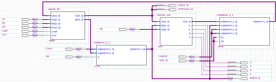
module datapath(C, V, N, Z, MA, MD, Op, AA, BA, DA, Load, Const, SB, SD, PORTA, PORTB, CLK);
   output C;            // Carry status bit.
   output V;            // oVerflow status bit.
   output N;            // Negative status bit.
   output Z;            // Zero status bit.
   output [15:0] MA;    // Memory address.
   inout [15:0]  MD;    // Memory data.
   input [3:0] 	 Op;    // Operation code.
   input [2:0] 	 AA;    // Address of A reg.
   input [2:0] 	 BA;    // Address of B reg.
   input [2:0] 	 DA;    // Address of C reg.
   input 	 Load;  // Enable loading of D reg - active high.
   input [15:0]  Const; // Constant.
   input 	 SB;    // Muxb selector.
   input [1:0]	 SD;    // Muxd selector.
   output [15:0] PORTA; // Port A.
   input [15:0]  PORTB; // Port B.
   input 	 CLK;   // Clock.

   wire [15:0] A;
   wire [15:0] B0;
   wire [15:0] B1;
   wire [15:0] D;
   wire [15:0] Y;

   assign MA = A;
   assign MD = (SD == 1'b0) ? B1 : 16'bz;
   assign PORTA = A;
   register_file regfile(A, B0, D, AA, BA, DA, Load, CLK);
   function_unit funit(Y, C, V, N, Z, A, B1, Op);
   multiplexer_2_1 muxb(B1, B0, Const, SB);
   multiplexer_4_1 muxd(D, Y, MD, PORTB, PORTB, SD[1], SD[0]);
endmodule // datapath
Register File
The design of this block is the same as the one found in the notes for the register file. It is a collection of eight 16-bit registers with output paths for two source registers, and an input path for one destination register.
module register_file(A, B, D, AA, BA, DA, Load, CLK);
   output [15:0] A;     // Data contents of A reg.
   output [15:0] B;     // Data contents of B reg.
   input [15:0]  D;     // Data to load into D reg.
   input [2:0] 	 AA;    // Address of A reg.
   input [2:0] 	 BA;    // Address of B reg.
   input [2:0] 	 DA;    // Address of C reg.
   input 	 Load;  // Enable loading of D reg - active high.
   input 	 CLK;   // Clock.

   wire [15:0] 	 Q0, Q1, Q2, Q3, Q4, Q5, Q6, Q7;
   wire 	 dr0, dr1, dr2, dr3, dr4, dr5, dr6,dr7;
   wire 	 load0, load1, load2, load3, load4, load5, load6, load7;

   multiplexer_8_1 muxa(A, Q0, Q1, Q2, Q3, Q4, Q5, Q6, Q7, AA);
   multiplexer_8_1 muxb(B, Q0, Q1, Q2, Q3, Q4, Q5, Q6, Q7, BA);

   octal_decoder decd(dr0, dr1, dr2, dr3, dr4, dr5, dr6, dr7, DA[2], DA[1], DA[0], 1'b1);

   and(load0, dr0, Load);
   and(load1, dr1, Load);
   and(load2, dr2, Load);
   and(load3, dr3, Load);
   and(load4, dr4, Load);
   and(load5, dr5, Load);
   and(load6, dr6, Load);
   and(load7, dr7, Load);

   register_parallel_load r0(Q0, D, load0, CLK);
   register_parallel_load r1(Q1, D, load1, CLK);
   register_parallel_load r2(Q2, D, load2, CLK);
   register_parallel_load r3(Q3, D, load3, CLK);
   register_parallel_load r4(Q4, D, load4, CLK);
   register_parallel_load r5(Q5, D, load5, CLK);
   register_parallel_load r6(Q6, D, load6, CLK);
   register_parallel_load r7(Q7, D, load7, CLK);
endmodule // register_file

module register_parallel_load(Q, D, Load, CLK);
   output [15:0] Q;
   input [15:0]  D;
   input 	 Load;
   input 	 CLK;

   wire 	 Loadn;
   wire 	 w1, w2, w3, w4, w5, w6, w7, w8, w9, w10, w11, w12;           // Connecting wires.
   wire 	 w13, w14, w15, w16, w17, w18, w19, w20, w21, w22, w23, w24;  // Connecting wires.
   wire 	 w25, w26, w27, w28, w29, w30, w31, w32, w33, w34, w35, w36;  // Connecting wires.
   wire 	 w37, w38, w39, w40, w41, w42, w43, w44, w45, w46, w47, w48;  // Connecting wires.
   wire [15:0] 	 Qn;   // Unused.

   not(Loadn, Load);

   and(w1, Q[0], Loadn);
   and(w2, D[0], Load);
   or(w3, w2, w1);

   and(w4, Q[1], Loadn);
   and(w5, D[1], Load);
   or(w6, w5, w4);

   and(w7, Q[2], Loadn);
   and(w8, D[2], Load);
   or(w9, w8, w7);

   and(w10, Q[3], Loadn);
   and(w11, D[3], Load);
   or(w12, w11, w10);

   and(w13, Q[4], Loadn);
   and(w14, D[4], Load);
   or(w15, w14, w13);

   and(w16, Q[5], Loadn);
   and(w17, D[5], Load);
   or(w18, w17, w16);

   and(w19, Q[6], Loadn);
   and(w20, D[6], Load);
   or(w21, w20, w19);

   and(w22, Q[7], Loadn);
   and(w23, D[7], Load);
   or(w24, w23, w22);

   and(w25, Q[8], Loadn);
   and(w26, D[8], Load);
   or(w27, w26, w25);

   and(w28, Q[9], Loadn);
   and(w29, D[9], Load);
   or(w30, w29, w28);

   and(w31, Q[10], Loadn);
   and(w32, D[10], Load);
   or(w33, w32, w31);

   and(w34, Q[11], Loadn);
   and(w35, D[11], Load);
   or(w36, w35, w34);

   and(w37, Q[12], Loadn);
   and(w38, D[12], Load);
   or(w39, w38, w37);

   and(w40, Q[13], Loadn);
   and(w41, D[13], Load);
   or(w42, w41, w40);

   and(w43, Q[14], Loadn);
   and(w44, D[14], Load);
   or(w45, w44, w43);

   and(w46, Q[15], Loadn);
   and(w47, D[15], Load);
   or(w48, w47, w46);

   d_flip_flop_edge_triggered dff0(Q[0], Qn[0], CLK, w3);
   d_flip_flop_edge_triggered dff1(Q[1], Qn[1], CLK, w6);
   d_flip_flop_edge_triggered dff2(Q[2], Qn[2], CLK, w9);
   d_flip_flop_edge_triggered dff3(Q[3], Qn[3], CLK, w12);
   d_flip_flop_edge_triggered dff4(Q[4], Qn[4], CLK, w15);
   d_flip_flop_edge_triggered dff5(Q[5], Qn[5], CLK, w18);
   d_flip_flop_edge_triggered dff6(Q[6], Qn[6], CLK, w21);
   d_flip_flop_edge_triggered dff7(Q[7], Qn[7], CLK, w24);
   d_flip_flop_edge_triggered dff8(Q[8], Qn[8], CLK, w27);
   d_flip_flop_edge_triggered dff9(Q[9], Qn[9], CLK, w30);
   d_flip_flop_edge_triggered dff10(Q[10], Qn[10], CLK, w33);
   d_flip_flop_edge_triggered dff11(Q[11], Qn[11], CLK, w36);
   d_flip_flop_edge_triggered dff12(Q[12], Qn[12], CLK, w39);
   d_flip_flop_edge_triggered dff13(Q[13], Qn[13], CLK, w42);
   d_flip_flop_edge_triggered dff14(Q[14], Qn[14], CLK, w45);
   d_flip_flop_edge_triggered dff15(Q[15], Qn[15], CLK, w48);

endmodule // register_parallel_load

module d_flip_flop_edge_triggered(Q, Qn, C, D);
   output Q;
   output Qn;
   input  C;
   input  D;

   wire   Cn;   // Control input to the D latch.
   wire   Cnn;  // Control input to the SR latch.
   wire   DQ;   // Output from the D latch, inputs to the gated SR latch.
   wire   DQn;  // Output from the D latch, inputs to the gated SR latch.

   not(Cn, C);
   not(Cnn, Cn);
   d_latch dl(DQ, DQn, Cn, D);
   sr_latch_gated sr(Q, Qn, Cnn, DQ, DQn);
endmodule // d_flip_flop_edge_triggered

module d_latch(Q, Qn, G, D);
   output Q;
   output Qn;
   input  G;
   input  D;

   wire   Dn;
   wire   D1;
   wire   Dn1;

   not(Dn, D);
   and(D1, G, D);
   and(Dn1, G, Dn);
   nor(Qn, D1, Q);
   nor(Q, Dn1, Qn);
endmodule // d_latch

module sr_latch_gated(Q, Qn, G, S, R);
   output Q;
   output Qn;
   input  G;
   input  S;
   input  R;

   wire   S1;
   wire   R1;

   and(S1, G, S);
   and(R1, G, R);
   nor(Qn, S1, Q);
   nor(Q, R1, Qn);
endmodule // sr_latch_gated

module octal_decoder(X0, X1, X2, X3, X4, X5, X6, X7, A2, A1, A0, E);
   output X0; // Minterm 0
   output X1; // Minterm 1
   output X2; // Minterm 2
   output X3; // Minterm 3
   output X4; // Minterm 4
   output X5; // Minterm 5
   output X6; // Minterm 6
   output X7; // Minterm 7

   input  A2;  // Input binary code most significant bit
   input  A1;  // Input binary code middle bit
   input  A0;  // Input binary code least significant bit

   input  E;   // Enable signal

   wire   A2n; // A2 negated
   wire   A1n; // A1 negated
   wire   A0n; // A0 negated

   not(A2n, A2);
   not(A1n, A1);
   not(A0n, A0);

   and(X0, A2n, A1n, A0n, E);  // Minterm 0: 000
   and(X1, A2n, A1n, A0, E);   // Minterm 1: 001
   and(X2, A2n, A1, A0n, E);   // Minterm 2: 010
   and(X3, A2n, A1, A0, E);    // Minterm 3: 011
   and(X4, A2, A1n, A0n, E);   // Minterm 4: 100
   and(X5, A2, A1n, A0, E);    // Minterm 5: 101
   and(X6, A2, A1, A0n, E);    // Minterm 6: 110
   and(X7, A2, A1, A0, E);     // Minterm 7: 111
endmodule // octal_decoder
Function Unit
The design of this block is the same as that found in the notes for the function unit.
module function_unit(Y, C, V, N, Z, A, B, Op);
   output [15:0] Y;  // Result.
   output 	 C;  // Carry.
   output 	 N;  // Negative.
   output 	 V;  // Overflow.
   output 	 Z;  // Zero.
   input [15:0]  A;  // Operand.
   input [15:0]  B;  // Operand.
   input [3:0] 	 Op; // Operation.

   wire [15:0] 	 Ya; // ALU result output.
   wire [15:0] 	 Ys; // Shifter result output.

   alu aluf(Ya, C, V, N, Z, A, B, {Op[2], Op[1], Op[0]});
   shifter_16 shifterf(Ys, A, {Op[1], Op[0]}, 1'b0, 1'b0);
   multiplexer_2_1 muxf(Y, Ya, Ys, Op[3]);
endmodule // function_unit
Shifter
The design of this block is the same as that found in the notes for the shifter.
module shifter_16(Y, A, S, L, R);
   output [15:0] Y;  // The shifted result.
   input [15:0]  A;  // The value to be shifted.
   input [1:0] 	 S;  // The direction of the shift.
   input 	 L;  // The leftmost bit to shift in.
   input 	 R;  // The rightmost bit to shift in.

   multiplexer_4_1 #(1) mux0(Y[0], A[0], A[1], L, 1'b0, S[1], S[0]);
   multiplexer_4_1 #(1) mux1(Y[1], A[1], A[2], A[0], 1'b0, S[1], S[0]);
   multiplexer_4_1 #(1) mux2(Y[2], A[2], A[3], A[1], 1'b0, S[1], S[0]);
   multiplexer_4_1 #(1) mux3(Y[3], A[3], A[4], A[2], 1'b0, S[1], S[0]);
   multiplexer_4_1 #(1) mux4(Y[4], A[4], A[5], A[3], 1'b0, S[1], S[0]);
   multiplexer_4_1 #(1) mux5(Y[5], A[5], A[6], A[4], 1'b0, S[1], S[0]);
   multiplexer_4_1 #(1) mux6(Y[6], A[6], A[7], A[5], 1'b0, S[1], S[0]);
   multiplexer_4_1 #(1) mux7(Y[7], A[7], A[8], A[6], 1'b0, S[1], S[0]);
   multiplexer_4_1 #(1) mux8(Y[8], A[8], A[9], A[7], 1'b0, S[1], S[0]);
   multiplexer_4_1 #(1) mux9(Y[9], A[9], A[10], A[8], 1'b0, S[1], S[0]);
   multiplexer_4_1 #(1) mux10(Y[10], A[10], A[11], A[9], 1'b0, S[1], S[0]);
   multiplexer_4_1 #(1) mux11(Y[11], A[11], A[12], A[10], 1'b0, S[1], S[0]);
   multiplexer_4_1 #(1) mux12(Y[12], A[12], A[13], A[11], 1'b0, S[1], S[0]);
   multiplexer_4_1 #(1) mux13(Y[13], A[13], A[14], A[12], 1'b0, S[1], S[0]);
   multiplexer_4_1 #(1) mux14(Y[14], A[14], A[15], A[13], 1'b0, S[1], S[0]);
   multiplexer_4_1 #(1) mux15(Y[15], A[15], R, A[14], 1'b0, S[1], S[0]);
endmodule // shifter_16
ALU
The design of this block is the same as that found in the notes for the ALU.
module alu(Y, C, V, N, Z, A, B, Op);
   output [15:0] Y;  // Result.
   output 	 C;  // Carry.
   output 	 N;  // Negative.
   output 	 V;  // Overflow.
   output 	 Z;  // Zero.
   input [15:0]  A;  // Operand.
   input [15:0]  B;  // Operand.
   input [2:0] 	 Op; // Operation.

   wire [15:0] 	 AS, And, Or, Xor, Not;
   wire 	 s;
   wire 	 Vas;
   wire 	 Cas;

   // The operations
   carry_select_adder_subtractor addsub(AS, Cas, Vas, A, B, Op[0]);      // Op == 3'b000, 3'b001
   andop aluand(And, A, B);                                              // Op == 3'b010
   orop aluor(Or, A, B);                                                 // Op == 3'b011
   xorop aluxor(Xor, A, B);                                              // Op == 3'b100
   notop alunot(Not, A);                                                 // Op == 3'b101
   multiplexer_8_1 muxy(Y, AS, AS, And, Or, Xor, Not, 16'b0, 16'b0, Op); // Select the result.

   nor(s, Op[1], Op[2]);   // s == 0 => a logical operation, otherwise and arithmetic operation.
   and(C, Cas, s);
   and(V, Vas, s);
   and(N, Y[15], s);       // Most significant bit is the sign bit in 2's complement.
   zero z(Z, Y);           // All operations can set the Zero status bit.
endmodule // alu

module andop(Y, A, B);
   output [15:0] Y;  // Result.
   input [15:0]  A;  // Operand.
   input [15:0]  B;  // Operand.

   and(Y[0], A[0], B[0]);
   and(Y[1], A[1], B[1]);
   and(Y[2], A[2], B[2]);
   and(Y[3], A[3], B[3]);
   and(Y[4], A[4], B[4]);
   and(Y[5], A[5], B[5]);
   and(Y[6], A[6], B[6]);
   and(Y[7], A[7], B[7]);
   and(Y[8], A[8], B[8]);
   and(Y[9], A[9], B[9]);
   and(Y[10], A[10], B[10]);
   and(Y[11], A[11], B[11]);
   and(Y[12], A[12], B[12]);
   and(Y[13], A[13], B[13]);
   and(Y[14], A[14], B[14]);
   and(Y[15], A[15], B[15]);
endmodule // andop

module orop(Y, A, B);
   output [15:0] Y; // Result.
   input [15:0]  A; // Operand.
   input [15:0]  B; // Operand.

   or(Y[0], A[0], B[0]);
   or(Y[1], A[1], B[1]);
   or(Y[2], A[2], B[2]);
   or(Y[3], A[3], B[3]);
   or(Y[4], A[4], B[4]);
   or(Y[5], A[5], B[5]);
   or(Y[6], A[6], B[6]);
   or(Y[7], A[7], B[7]);
   or(Y[8], A[8], B[8]);
   or(Y[9], A[9], B[9]);
   or(Y[10], A[10], B[10]);
   or(Y[11], A[11], B[11]);
   or(Y[12], A[12], B[12]);
   or(Y[13], A[13], B[13]);
   or(Y[14], A[14], B[14]);
   or(Y[15], A[15], B[15]);
endmodule // orop

module xorop(Y, A, B);
   output [15:0] Y; // Result.
   input [15:0]  A; // Operand.
   input [15:0]  B; // Operand.

   xor(Y[0], A[0], B[0]);
   xor(Y[1], A[1], B[1]);
   xor(Y[2], A[2], B[2]);
   xor(Y[3], A[3], B[3]);
   xor(Y[4], A[4], B[4]);
   xor(Y[5], A[5], B[5]);
   xor(Y[6], A[6], B[6]);
   xor(Y[7], A[7], B[7]);
   xor(Y[8], A[8], B[8]);
   xor(Y[9], A[9], B[9]);
   xor(Y[10], A[10], B[10]);
   xor(Y[11], A[11], B[11]);
   xor(Y[12], A[12], B[12]);
   xor(Y[13], A[13], B[13]);
   xor(Y[14], A[14], B[14]);
   xor(Y[15], A[15], B[15]);
endmodule // xorop

module notop(Y, A);
   output [15:0] Y; // Result.
   input [15:0]  A; // Operand.

   not(Y[0], A[0]);
   not(Y[1], A[1]);
   not(Y[2], A[2]);
   not(Y[3], A[3]);
   not(Y[4], A[4]);
   not(Y[5], A[5]);
   not(Y[6], A[6]);
   not(Y[7], A[7]);
   not(Y[8], A[8]);
   not(Y[9], A[9]);
   not(Y[10], A[10]);
   not(Y[11], A[11]);
   not(Y[12], A[12]);
   not(Y[13], A[13]);
   not(Y[14], A[14]);
   not(Y[15], A[15]);
endmodule // notop

module zero(Z, A);
   output Z;        // Result.
   input [15:0]  A; // Operand.

   wire [15:0] 	 Y; // Temp result.

   xnor(Y[0], A[0], 1'b0);
   xnor(Y[1], A[1], 1'b0);
   xnor(Y[2], A[2], 1'b0);
   xnor(Y[3], A[3], 1'b0);
   xnor(Y[4], A[4], 1'b0);
   xnor(Y[5], A[5], 1'b0);
   xnor(Y[6], A[6], 1'b0);
   xnor(Y[7], A[7], 1'b0);
   xnor(Y[8], A[8], 1'b0);
   xnor(Y[9], A[9], 1'b0);
   xnor(Y[10], A[10], 1'b0);
   xnor(Y[11], A[11], 1'b0);
   xnor(Y[12], A[12], 1'b0);
   xnor(Y[13], A[13], 1'b0);
   xnor(Y[14], A[14], 1'b0);
   xnor(Y[15], A[15], 1'b0);
   and(Z, Y[0], Y[1], Y[2], Y[3], Y[4],
       Y[5], Y[6], Y[7], Y[8],
       Y[9], Y[10], Y[11], Y[12],
       Y[13], Y[14], Y[15]);
endmodule // zero

module carry_select_adder_subtractor(S, C, V, A, B, Op);
   output [15:0] S;   // The 16-bit sum/difference.
   output 	 C;   // The 1-bit carry/borrow status.
   output 	 V;   // The 1-bit overflow status.
   input [15:0]  A;   // The 16-bit augend/minuend.
   input [15:0]  B;   // The 16-bit addend/subtrahend.
   input 	 Op;  // The operation: 0 => Add, 1=>Subtract.

   wire 	 C15; // The carry out bit of adder/subtractor, used to generate final carry/borrrow.
   wire [15:0] 	 Bx;

   // Looking at the truth table for not we see that
   // B xor 0 = B, and
   // B xor 1 = not(B).
   // So, if Op==1 means we are subtracting, then
   // adding A and B xor Op alog with setting the first
   // carry bit to Op, will give us a result of
   // A+B when Op==0, and A+not(B)+1 when Op==1.
   // Note that not(B)+1 is the 2's complement of B, so
   // this gives us subtraction.
   xor(Bx[0], B[0], Op);
   xor(Bx[1], B[1], Op);
   xor(Bx[2], B[2], Op);
   xor(Bx[3], B[3], Op);
   xor(Bx[4], B[4], Op);
   xor(Bx[5], B[5], Op);
   xor(Bx[6], B[6], Op);
   xor(Bx[7], B[7], Op);
   xor(Bx[8], B[8], Op);
   xor(Bx[9], B[9], Op);
   xor(Bx[10], B[10], Op);
   xor(Bx[11], B[11], Op);
   xor(Bx[12], B[12], Op);
   xor(Bx[13], B[13], Op);
   xor(Bx[14], B[14], Op);
   xor(Bx[15], B[15], Op);
   xor(C, C15, Op);            // Carry = C15 for addition, Carry = not(C15) for subtraction.
   carry_select_adder csa(S, C15, V, A, Bx, Op);
endmodule // carry_select_adder_subtractor

module carry_select_adder(S, C, V, A, B, Cin);
   output [15:0] S;   // The 16-bit sum.
   output 	 C;   // The 1-bit carry.
   output 	 V;   // The 1-bit overflow status.
   input [15:0]  A;   // The 16-bit augend.
   input [15:0]  B;   // The 16-bit addend.
   input 	 Cin; // The initial carry in.

   wire [3:0] 	S1_0;   // Nibble 1 sum output with carry input 0.
   wire [3:0] 	S1_1;   // Nibble 1 sum output with carry input 1.
   wire [3:0] 	S2_0;   // Nibble 2 sum output with carry input 0.
   wire [3:0] 	S2_1;   // Nibble 2 sum output with carry input 1.
   wire [3:0] 	S3_0;   // Nibble 3 sum output with carry input 0.
   wire [3:0] 	S3_1;   // Nibble 3 sum output with carry input 1.
   wire 	C1_0;   // Nibble 1 carry output with carry input 0.
   wire 	C1_1;   // Nibble 1 carry output with carry input 1.
   wire 	C2_0;   // Nibble 2 carry output with carry input 0.
   wire 	C2_1;   // Nibble 2 carry output with carry input 1.
   wire 	C3_0;   // Nibble 3 carry output with carry input 0.
   wire 	C3_1;   // Nibble 3 carry output with carry input 1.
   wire 	C0;     // Nibble 0 carry output used to select multiplexer output.
   wire 	C1;     // Nibble 1 carry output used to select multiplexer output.
   wire 	C2;     // Nibble 2 carry output used to select multiplexer output.
   wire         V0;     // Nibble 0 overflow output.
   wire 	V1_0;   // Nibble 1 overflow output with carry input 0.
   wire 	V1_1;   // Nibble 1 overflow output with carry input 1.
   wire 	V2_0;   // Nibble 2 overflow output with carry input 0.
   wire 	V2_1;   // Nibble 2 overflow output with carry input 1.
   wire 	V3_0;   // Nibble 3 overflow output with carry input 0.
   wire 	V3_1;   // Nibble 3 overflow output with carry input 1.

   ripple_carry_adder rc_nibble_0(S[3:0], C0, V0, A[3:0], B[3:0], Cin);          // Calculate S nibble 0.
   ripple_carry_adder rc_nibble_1_carry_0(S1_0, C1_0, V1_0, A[7:4], B[7:4], 1'b0);      // Calculate S nibble 1 with carry input 0.
   ripple_carry_adder rc_nibble_1_carry_1(S1_1, C1_1, V1_1, A[7:4], B[7:4], 1'b1);      // Calculate S nibble 1 with carry input 1.
   ripple_carry_adder rc_nibble_2_carry_0(S2_0, C2_0, V2_0, A[11:8], B[11:8], 1'b0);    // Calculate S nibble 2 with carry input 0.
   ripple_carry_adder rc_nibble_2_carry_1(S2_1, C2_1, V2_1, A[11:8], B[11:8], 1'b1);    // Calculate S nibble 2 with carry input 1.
   ripple_carry_adder rc_nibble_3_carry_0(S3_0, C3_0, V3_0, A[15:12], B[15:12], 1'b0);  // Calculate S nibble 3 with carry input 0.
   ripple_carry_adder rc_nibble_3_carry_1(S3_1, C3_1, V3_1, A[15:12], B[15:12], 1'b1);  // Calculate S nibble 3 with carry input 1.

   multiplexer_2_1 #(1) muxc1(C1, C1_0, C1_1, C0); // C0 selects the carry output for nibble 1.
   multiplexer_2_1 #(1) muxc2(C2, C2_0, C2_1, C1); // C1 selects the carry output for nibble 2.
   multiplexer_2_1 #(1) muxc(C, C3_0, C3_1, C2);   // C2 selects the carry output for nibble 3 which is the global carry output.
   multiplexer_2_1 #(1) muxv(V, V3_0, V3_1, C2);   // C2 selects the overflow output for nibble 3 which is the global overflow output.

   multiplexer_2_1 #(4) muxs1(S[7:4], S1_0, S1_1, C0);    // C0 selects the result for nibble 1.
   multiplexer_2_1 #(4) muxs2(S[11:8], S2_0, S2_1, C1);   // C1 selects the result for nibble 2.
   multiplexer_2_1 #(4) muxs3(S[15:12], S3_0, S3_1, C2);  // C2 selects the result for nibble 3.
endmodule // carry_select_adder

module ripple_carry_adder(S, C, V, A, B, Cin);
   output [3:0] S;   // The 4-bit sum.
   output 	C;   // The 1-bit carry.
   output       V;   // The 1-bit overflow status.
   input [3:0] 	A;   // The 4-bit augend.
   input [3:0] 	B;   // The 4-bit addend.
   input 	Cin; // The carry input.

   wire 	C0; // The carry out bit of fa0, the carry in bit of fa1.
   wire 	C1; // The carry out bit of fa1, the carry in bit of fa2.
   wire 	C2; // The carry out bit of fa2, the carry in bit of fa3.

   full_adder fa0(S[0], C0, A[0], B[0], Cin);    // Least significant bit.
   full_adder fa1(S[1], C1, A[1], B[1], C0);
   full_adder fa2(S[2], C2, A[2], B[2], C1);
   full_adder fa3(S[3], C, A[3], B[3], C2);    // Most significant bit.
   xor(V, C, C2);  // Overflow
endmodule // ripple_carry_adder

module full_adder(S, Cout, A, B, Cin);
   output S;
   output Cout;
   input  A;
   input  B;
   input  Cin;

   wire   w1;
   wire   w2;
   wire   w3;
   wire   w4;

   xor(w1, A, B);
   xor(S, Cin, w1);
   and(w2, A, B);
   and(w3, A, Cin);
   and(w4, B, Cin);
   or(Cout, w2, w3, w4);
endmodule // full_adder
RAM
We don't use the RAM on the board but just create it on the FPGA. The design is taken from the notes for RAM.
module ram (data, addr, en, wr, clk);
   inout [15:0]                   data;   // Data bus.
   input [15:0] 		  addr;   // Address bus.
   input 			  clk;    // We perform action on +ve edge of this clock.
   input 			  en;     // Device enable
   input 			  wr;     // wr = 1 => write, wr = 0 => read.
   wire [15:0] 			  odata;  // Used to drive the data bus.
   reg [15:0] 			  memory[0:256];

   assign data = (en && !wr) ? odata : 16'bz;
   assign odata = memory[addr];
   always @(posedge clk)
     begin
        if(en && wr)
	  begin
	     memory[addr] <= data;
	  end
     end
endmodule // ram
Port A
The output port sends the four least significant bits of its data contents to the four LEDs on the board.
module porta (leds, data, en, clk);
   output[3:0] leds;
   input [15:0] data;   // Data to write to the leds.
   input 	en;     // Port enable.
   input 	clk;

   reg [15:0] 	port;

   assign leds[0] = port[0];
   assign leds[1] = port[1];
   assign leds[2] = port[2];
   assign leds[3] = port[3];

   always @(posedge clk)
     begin
        if(en)
	  begin
	     port <= data;
	  end
     end
endmodule // porta
Port B
The input port just outputs the contents of the four push buttons on every clock cycle.
module portb (data, buttons, clk);
   output [15:0] data;   // Data read from buttons.
   input [3:0] 	buttons;
   input 	clk;

   reg [15:0] 	data;

   always @(posedge clk)
     begin
	data[0] <= buttons[0];
	data[1] <= buttons[1];
	data[2] <= buttons[2];
	data[3] <= buttons[3];
	data[15:4] <= 12'b000000000000;
     end
endmodule // portb
Multiplexer
The design of this block is the same as that found in the notes for the multiplexer.
module multiplexer_2_1(X, A0, A1, S);
   parameter WIDTH=16;     // How many bits wide are the lines

   output [WIDTH-1:0] X;   // The output line

   input [WIDTH-1:0]  A1;  // Input line with id 1'b1
   input [WIDTH-1:0]  A0;  // Input line with id 1'b0
   input 	      S;  // Selection bit

   assign X = (S == 1'b0) ? A0 : A1;
endmodule // multiplexer_2_1

module multiplexer_4_1(X, A0, A1, A2, A3, S1, S0);
   parameter WIDTH=16;     // How many bits wide are the lines

   output [WIDTH-1:0] X;   // The output line

   input [WIDTH-1:0]  A3;  // Input line with id 2'b11
   input [WIDTH-1:0]  A2;  // Input line with id 2'b10
   input [WIDTH-1:0]  A1;  // Input line with id 2'b01
   input [WIDTH-1:0]  A0;  // Input line with id 2'b00
   input 	      S0;  // Least significant selection bit
   input 	      S1;  // Most significant selection bit

   assign X = (S1 == 0
	       ? (S0 == 0
		  ? A0       // {S1,S0} = 2'b00
		  : A1)      // {S1,S0} = 2'b01
	       : (S0 == 0
		  ? A2       // {S1,S0} = 2'b10
		  : A3));    // {S1,S0} = 2'b11
endmodule // multiplexer_4_1

module multiplexer_8_1(X, A0, A1, A2, A3, A4, A5, A6, A7, S);
   parameter WIDTH=16;     // How many bits wide are the lines

   output [WIDTH-1:0] X;   // The output line

   input [WIDTH-1:0]  A7;  // Input line with id 3'b111
   input [WIDTH-1:0]  A6;  // Input line with id 3'b110
   input [WIDTH-1:0]  A5;  // Input line with id 3'b101
   input [WIDTH-1:0]  A4;  // Input line with id 3'b100
   input [WIDTH-1:0]  A3;  // Input line with id 3'b011
   input [WIDTH-1:0]  A2;  // Input line with id 3'b010
   input [WIDTH-1:0]  A1;  // Input line with id 3'b001
   input [WIDTH-1:0]  A0;  // Input line with id 3'b000
   input [2:0]	      S;

   assign X = (S[2] == 0
	       ? (S[1] == 0
		  ? (S[0] == 0
		     ? A0       // {S2,S1,S0} = 3'b000
		     : A1)      // {S2,S1,S0} = 3'b001
		  : (S[0] == 0
		     ? A2       // {S2,S1,S0} = 3'b010
		     : A3))     // {S2,S1,S0} = 3'b011
	       : (S[1] == 0
		  ? (S[0] == 0
		     ? A4       // {S2,S1,S0} = 3'b100
		     : A5)      // {S2,S1,S0} = 3'b101
		  : (S[0] == 0
		     ? A6       // {S2,S1,S0} = 3'b110
		     : A7)));   // {S2,S1,S0} = 3'b111
endmodule // multiplexer_8_1
References
Mano, M. Morris, and Kime, Charles R. Logic and Computer Design Fundamentals. 2nd Edition. Prentice Hall, 2000.