Microprogrammed Nonprogrammable Control Unit Design Example (Greatest Common Divisor)
The following is an example of an algorithmic state machine (ASM) being used to design a microprogrammed nonprogrammable control unit.
Problem Description
We want to calculate the greatest common divisor (gcd) of two positive integers. The mathematical specification of the gcd function is shown below:
gcd(a,a) = a
gcd(a,b) = gcd(a-b, b)    if a>b,
gcd(a,b) = gcd(a, b-a)    otherwise.
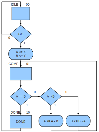
Algorithmic State Machine
The first step is converting the mathematical specification into an ASM.
The following is just such an ASM.
It comprises three states (IDLE, COMP, and DONE),
two registers (A and B),
three inputs (X, Y, and GO),
and two outputs (DONE and either A or B — let's choose A).
If the initial state is IDLE and the arguments of the gcd function are X and Y, then gcd(X,Y)
will eventually be loaded into A.
The input GO starts the whole process, and the output DONE is pulsed (0 to 1) when
A contains the result.
This would be fine for a hardwired control unit, but for a microprogrammed unit, we need to remove the ASM's conditional outputs as we need a Moore model. The simplest way to do this is to replace all conditional outputs with new states as shown below:
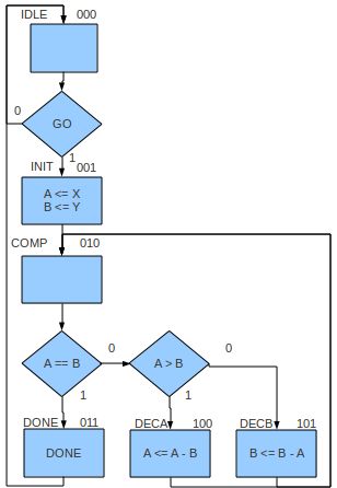
It now comprises six states (IDLE, INIT, COMP, DECA, DECB, and DONE).
This increase in the number of states will impact computation time as each state transition takes a clock period.
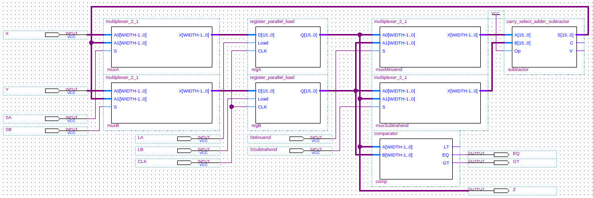
Datapath
Analysing the ASM we see that any destination of a register transfer will need to be a register,
so we need registers A and B.
The RTL operations performed give us the
combinational logic circuits needed.
In this case we need a subtractor.
From analysing the decisions in the ASM we also need a comparator which can signal "equal" and "greater than".
A 16-bit wide datapath derived from the ASM is shown in schematic form below (the WIDTH parameter used in some blocks
should be 16). The output Z is the result of the calculation.
Control Store
We'll use a ROM to implement the control store.
We'll store the microinstruction for the state with binary code X at address X, i.e., DECA has its microinstruction
at address 100 (decimal 4).
We have six states so we will need six addresses, therefore a ROM address will comprise three bits
(22=4 < 6 < 23=8).
We'll also encode the next microinstruction address in the current microinstruction being executed.
This means that the instruction will need an address to jump to for each possible combination of the three condition inputs
(GO, EQ and GT).
Consequently each instruction will need to contain 8 (23) addresses and since each address is three bits, we'll need
24 bits just for addresses.
Looking at the ASM we see that we can get away with less than half of that.
In the instruction that checks GO we only need two addresses: the address to jump to on GO == 0 and the address to
jump to on GO == 1.
In the instruction that will compare A and B we only need three addresses:
EQ == 0 & GT == 0, EQ == 0 & GT == 1, and EQ == 1 & GT == 0.
Since we can't execute these two instructions at the same time we can get away with the worst case which is three target addresses, so we need only
9 bits for addresses.
We'll call these three target addresses Next00, Next01, and Next10.
We'll also use a signal SEL to tell us how to interpret these three addresses.
This is all summarised in the table below:
SEL |
Next00 | Next01 | Next10 |
|---|---|---|---|
0 |
GO == 0 |
GO == 1 |
Unused |
1 |
EQ == 0 & GT == 0 |
EQ == 0 & GT == 1 |
EQ == 1 & GT == 0 |
For the datapath control signalling we need six bits:
LA, LB, SA, SB, SMinuend, and SSubtrahend.
These control signals are Moore outputs so they depend only upon control unit state (or current control store address).
For the control unit output we need only one bit:
DONE.
Again, this is a Moore output that only depends upon control unit state (or current control store address).
We can now specify the control store as shown in the table below. As can be seen the control store is 17 bits wide.
| Control Word | |||||||||||
|---|---|---|---|---|---|---|---|---|---|---|---|
| Target Addresses | Datapath Control | Control Unit Output | |||||||||
| Address | Next00 | Next01 | Next10 | SEL | LA |
LB |
SA |
SB |
SMinuend |
SSubtrahend |
DONE |
000 |
000 | 001 | 000 |
1 |
0 | 0 | 0 | 0 | 0 | 0 |
0 |
001 |
010 | 010 | 010 |
1 |
1 | 1 | 0 | 0 | 0 | 0 |
0 |
010 |
101 | 100 | 011 |
0 |
0 | 0 | 0 | 0 | 0 | 0 |
0 |
011 |
000 | 000 | 000 |
0 |
0 | 0 | 0 | 0 | 0 | 0 |
1 |
100 |
010 | 010 | 010 |
0 |
1 | 0 | 1 | 0 | 0 | 0 |
0 |
101 |
010 | 010 | 010 |
0 |
0 | 1 | 0 | 1 | 1 | 1 |
0 |
The design described above can be combined with an input signal (RESETn) to reset the control store address to zero.
A schematic which implements all this is given below:
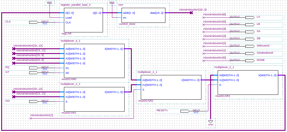
The register regCAR is the control address register used to address the microinstruction in the control store ROM.
The multiplexers muxCAR0, muxCAR1, muxCAR2, and muxCAR3 are used to load the
contents of regCAR with the next address.
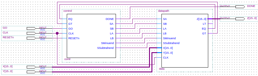
Top-level
Now we can fit the control unit and datapath together. At the highest level of abstraction, the design looks like this:
Implementation
The full Verilog code for the implementation of the design is shown below.
module gcd(Z, DONE, X, Y, GO, CLK, RESETn);
   output [15:0] Z;
   output 	 DONE;
   input [15:0]  X;
   input [15:0]  Y;
   input 	 GO;
   input 	 CLK;
   input 	 RESETn;

   datapath data(Z, LT, EQ, GT, SA, SB, LA, LB, SMinuend, SSubtrahend, X, Y, CLK);
   control contr(DONE, SA, SB, LA, LB, SMinuend, SSubtrahend, EQ, GT, GO, CLK, RESETn);
endmodule // gcd

module control(DONE, SA, SB, LA, LB, SMinuend, SSubtrahend, EQ, GT, GO, CLK, RESETn);
   output DONE;
   output SA;
   output SB;
   output LA;
   output LB;
   output SMinuend;
   output SSubtrahend;
   input  EQ;
   input  GT;
   input  GO;
   input  CLK;
   input  RESETn;


   wire [2:0] Next00;
   wire [2:0] Next01;
   wire [2:0] Next10;
   wire [2:0] Next11;
   wire       SEL;

   wire [16:0] microinstruction;
   wire [2:0]  DCAR0;
   wire [2:0]  DCAR1;
   wire [2:0]  DCAR2;
   wire [2:0]  DCAR;
   wire [2:0]  CAR;

   register_parallel_load_3 regCAR(CAR, DCAR, 1'b1, CLK);
   rom control_store(microinstruction, CAR, 1'b1);

   multiplexer_4_1 #(3)muxDCAR0(DCAR0, Next00, Next01, Next10, Next10, EQ, GT);
   multiplexer_2_1 #(3)muxDCAR1(DCAR1, Next00, Next01, GO);
   multiplexer_2_1 #(3)muxDCAR2(DCAR2, DCAR0, DCAR1, SEL);
   multiplexer_2_1 #(3)muxDCAR(DCAR, 3'b000, DCAR2, RESETn);

   assign Next00 = microinstruction[16:14];
   assign Next01 = microinstruction[13:11];
   assign Next10 = microinstruction[10:8];
   assign SEL = microinstruction[7];
   assign LA = microinstruction[6];
   assign LB = microinstruction[5];
   assign SA = microinstruction[4];
   assign SB = microinstruction[3];
   assign SMinuend = microinstruction[2];
   assign SSubtrahend = microinstruction[1];
   assign DONE = microinstruction[0];
endmodule // control

module rom (data, addr, en);
   output [16:0] data;
   input 	 en;
   input [2:0] 	 addr;

   wire [16:0] 	 odata;

   assign odata = (addr == 3'b000)   ? 17'b000_001_000_1_000000_0
		  : (addr == 3'b001) ? 17'b010_010_010_1_110000_0
		  : (addr == 3'b010) ? 17'b101_100_011_0_000000_0
		  : (addr == 3'b011) ? 17'b000_000_000_0_000000_1
		  : (addr == 3'b100) ? 17'b010_010_010_0_101000_0
		  : (addr == 3'b101) ? 17'b010_010_010_0_010111_0
		  : (addr == 3'b110) ? 17'b000_001_000_1_000000_0
		  : 17'b000_001_000_1_000000_0;
   assign data = en ? odata : 17'bz;
endmodule


module datapath(Z, LT, EQ, GT, SA, SB, LA, LB, SMinuend, SSubtrahend, X, Y, CLK);
   output [15:0] Z;
   output 	      LT;
   output 	      EQ;
   output 	      GT;
   input  	      SA;
   input  	      SB;
   input  	      LA;
   input  	      LB;
   input  	      SMinuend;
   input  	      SSubtrahend;
   input [15:0]  X;
   input [15:0]  Y;
   input 	      CLK;

   wire [15:0] 	      A;
   wire [15:0] 	      B;
   wire [15:0] 	      DA;
   wire [15:0] 	      DB;
   wire [15:0] 	      Minuend;
   wire [15:0] 	      Subtrahend;
   wire [15:0] 	      Difference;   // Difference = Minuend - Subtrahend
   wire 	      Borrow;
   wire 	      Overflow;

   assign Z=A;
   multiplexer_2_1 muxA1(DA, X, Difference, SA);
   multiplexer_2_1 muxB1(DB, Y, Difference, SB);
   register_parallel_load_16 regA(A, DA, LA, CLK);
   register_parallel_load_16 regB(B, DB, LB, CLK);
   multiplexer_2_1 muxMinuend(Minuend, A, B, SMinuend);
   multiplexer_2_1 muxSubtrahend(Subtrahend, B, A, SSubtrahend);
   comparator comp(LT, EQ, GT, A, B);
   carry_select_adder_subtractor subtractor(Difference, Borrow, Overflow, Minuend, Subtrahend, 1'b1);
endmodule // datapath


module comparator(LT, EQ, GT, A, B);
   parameter WIDTH=16;     // How many bits wide are the lines
   output LT;
   output EQ;
   output GT;
   input [WIDTH-1:0] A;
   input [WIDTH-1:0] B;

   assign LT = (A < B) ? 1 : 0;
   assign EQ = (A == B) ? 1 : 0;
   assign GT = ~LT & ~EQ;
endmodule // comparator

module register_parallel_load_3(Q, D, Load, CLK);
   output [2:0] Q;
   input [2:0] 	D;
   input 	Load;
   input 	CLK;

   wire 	Loadn;
   wire 	w1, w2, w3, w4, w5, w6, w7, w8, w9;           // Connecting wires.
   wire [2:0] 	Qn;   // Unused.

   not(Loadn, Load);

   and(w1, Q[0], Loadn);
   and(w2, D[0], Load);
   or(w3, w2, w1);

   and(w4, Q[1], Loadn);
   and(w5, D[1], Load);
   or(w6, w5, w4);

   and(w7, Q[2], Loadn);
   and(w8, D[2], Load);
   or(w9, w8, w7);

   d_flip_flop_edge_triggered dff0(Q[0], Qn[0], CLK, w3);
   d_flip_flop_edge_triggered dff1(Q[1], Qn[1], CLK, w6);
   d_flip_flop_edge_triggered dff2(Q[2], Qn[2], CLK, w9);
endmodule // register_parallel_load_3

module register_parallel_load_16(Q, D, Load, CLK);
   output [15:0] Q;
   input [15:0]  D;
   input 	 Load;
   input 	 CLK;

   wire 	 Loadn;
   wire 	 w1, w2, w3, w4, w5, w6, w7, w8, w9, w10, w11, w12;           // Connecting wires.
   wire 	 w13, w14, w15, w16, w17, w18, w19, w20, w21, w22, w23, w24;  // Connecting wires.
   wire 	 w25, w26, w27, w28, w29, w30, w31, w32, w33, w34, w35, w36;  // Connecting wires.
   wire 	 w37, w38, w39, w40, w41, w42, w43, w44, w45, w46, w47, w48;  // Connecting wires.
   wire [15:0] 	 Qn;   // Unused.

   not(Loadn, Load);

   and(w1, Q[0], Loadn);
   and(w2, D[0], Load);
   or(w3, w2, w1);

   and(w4, Q[1], Loadn);
   and(w5, D[1], Load);
   or(w6, w5, w4);

   and(w7, Q[2], Loadn);
   and(w8, D[2], Load);
   or(w9, w8, w7);

   and(w10, Q[3], Loadn);
   and(w11, D[3], Load);
   or(w12, w11, w10);

   and(w13, Q[4], Loadn);
   and(w14, D[4], Load);
   or(w15, w14, w13);

   and(w16, Q[5], Loadn);
   and(w17, D[5], Load);
   or(w18, w17, w16);

   and(w19, Q[6], Loadn);
   and(w20, D[6], Load);
   or(w21, w20, w19);

   and(w22, Q[7], Loadn);
   and(w23, D[7], Load);
   or(w24, w23, w22);

   and(w25, Q[8], Loadn);
   and(w26, D[8], Load);
   or(w27, w26, w25);

   and(w28, Q[9], Loadn);
   and(w29, D[9], Load);
   or(w30, w29, w28);

   and(w31, Q[10], Loadn);
   and(w32, D[10], Load);
   or(w33, w32, w31);

   and(w34, Q[11], Loadn);
   and(w35, D[11], Load);
   or(w36, w35, w34);

   and(w37, Q[12], Loadn);
   and(w38, D[12], Load);
   or(w39, w38, w37);

   and(w40, Q[13], Loadn);
   and(w41, D[13], Load);
   or(w42, w41, w40);

   and(w43, Q[14], Loadn);
   and(w44, D[14], Load);
   or(w45, w44, w43);

   and(w46, Q[15], Loadn);
   and(w47, D[15], Load);
   or(w48, w47, w46);

   d_flip_flop_edge_triggered dff0(Q[0], Qn[0], CLK, w3);
   d_flip_flop_edge_triggered dff1(Q[1], Qn[1], CLK, w6);
   d_flip_flop_edge_triggered dff2(Q[2], Qn[2], CLK, w9);
   d_flip_flop_edge_triggered dff3(Q[3], Qn[3], CLK, w12);
   d_flip_flop_edge_triggered dff4(Q[4], Qn[4], CLK, w15);
   d_flip_flop_edge_triggered dff5(Q[5], Qn[5], CLK, w18);
   d_flip_flop_edge_triggered dff6(Q[6], Qn[6], CLK, w21);
   d_flip_flop_edge_triggered dff7(Q[7], Qn[7], CLK, w24);
   d_flip_flop_edge_triggered dff8(Q[8], Qn[8], CLK, w27);
   d_flip_flop_edge_triggered dff9(Q[9], Qn[9], CLK, w30);
   d_flip_flop_edge_triggered dff10(Q[10], Qn[10], CLK, w33);
   d_flip_flop_edge_triggered dff11(Q[11], Qn[11], CLK, w36);
   d_flip_flop_edge_triggered dff12(Q[12], Qn[12], CLK, w39);
   d_flip_flop_edge_triggered dff13(Q[13], Qn[13], CLK, w42);
   d_flip_flop_edge_triggered dff14(Q[14], Qn[14], CLK, w45);
   d_flip_flop_edge_triggered dff15(Q[15], Qn[15], CLK, w48);

endmodule // register_parallel_load_16

module d_flip_flop_edge_triggered(Q, Qn, C, D);
   output Q;
   output Qn;
   input  C;
   input  D;

   wire   Cn;   // Control input to the D latch.
   wire   Cnn;  // Control input to the SR latch.
   wire   DQ;   // Output from the D latch, inputs to the gated SR latch.
   wire   DQn;  // Output from the D latch, inputs to the gated SR latch.

   not(Cn, C);
   not(Cnn, Cn);
   d_latch dl(DQ, DQn, Cn, D);
   sr_latch_gated sr(Q, Qn, Cnn, DQ, DQn);
endmodule // d_flip_flop_edge_triggered

module d_latch(Q, Qn, G, D);
   output Q;
   output Qn;
   input  G;
   input  D;

   wire   Dn;
   wire   D1;
   wire   Dn1;

   not(Dn, D);
   and(D1, G, D);
   and(Dn1, G, Dn);
   nor(Qn, D1, Q);
   nor(Q, Dn1, Qn);
endmodule // d_latch

module sr_latch_gated(Q, Qn, G, S, R);
   output Q;
   output Qn;
   input  G;
   input  S;
   input  R;

   wire   S1;
   wire   R1;

   and(S1, G, S);
   and(R1, G, R);
   nor(Qn, S1, Q);
   nor(Q, R1, Qn);
endmodule // sr_latch_gated

module carry_select_adder_subtractor(S, C, V, A, B, Op);
   output [15:0] S;   // The 16-bit sum/difference.
   output 	 C;   // The 1-bit carry/borrow status.
   output 	 V;   // The 1-bit overflow status.
   input [15:0]  A;   // The 16-bit augend/minuend.
   input [15:0]  B;   // The 16-bit addend/subtrahend.
   input 	 Op;  // The operation: 0 => Add, 1=>Subtract.

   wire 	 C15; // The carry out bit of adder/subtractor, used to generate final carry/borrrow.
   wire [15:0] 	 Bx;

   // Looking at the truth table for not we see that
   // B xor 0 = B, and
   // B xor 1 = not(B).
   // So, if Op==1 means we are subtracting, then
   // adding A and B xor Op alog with setting the first
   // carry bit to Op, will give us a result of
   // A+B when Op==0, and A+not(B)+1 when Op==1.
   // Note that not(B)+1 is the 2's complement of B, so
   // this gives us subtraction.
   xor(Bx[0], B[0], Op);
   xor(Bx[1], B[1], Op);
   xor(Bx[2], B[2], Op);
   xor(Bx[3], B[3], Op);
   xor(Bx[4], B[4], Op);
   xor(Bx[5], B[5], Op);
   xor(Bx[6], B[6], Op);
   xor(Bx[7], B[7], Op);
   xor(Bx[8], B[8], Op);
   xor(Bx[9], B[9], Op);
   xor(Bx[10], B[10], Op);
   xor(Bx[11], B[11], Op);
   xor(Bx[12], B[12], Op);
   xor(Bx[13], B[13], Op);
   xor(Bx[14], B[14], Op);
   xor(Bx[15], B[15], Op);
   xor(C, C15, Op);            // Carry = C15 for addition, Carry = not(C15) for subtraction.
   carry_select_adder csa(S, C15, V, A, Bx, Op);
endmodule // carry_select_adder_subtractor

module carry_select_adder(S, C, V, A, B, Cin);
   output [15:0] S;   // The 16-bit sum.
   output 	 C;   // The 1-bit carry.
   output 	 V;   // The 1-bit overflow status.
   input [15:0]  A;   // The 16-bit augend.
   input [15:0]  B;   // The 16-bit addend.
   input 	 Cin; // The initial carry in.

   wire [3:0] 	S1_0;   // Nibble 1 sum output with carry input 0.
   wire [3:0] 	S1_1;   // Nibble 1 sum output with carry input 1.
   wire [3:0] 	S2_0;   // Nibble 2 sum output with carry input 0.
   wire [3:0] 	S2_1;   // Nibble 2 sum output with carry input 1.
   wire [3:0] 	S3_0;   // Nibble 3 sum output with carry input 0.
   wire [3:0] 	S3_1;   // Nibble 3 sum output with carry input 1.
   wire 	C1_0;   // Nibble 1 carry output with carry input 0.
   wire 	C1_1;   // Nibble 1 carry output with carry input 1.
   wire 	C2_0;   // Nibble 2 carry output with carry input 0.
   wire 	C2_1;   // Nibble 2 carry output with carry input 1.
   wire 	C3_0;   // Nibble 3 carry output with carry input 0.
   wire 	C3_1;   // Nibble 3 carry output with carry input 1.
   wire 	C0;     // Nibble 0 carry output used to select multiplexer output.
   wire 	C1;     // Nibble 1 carry output used to select multiplexer output.
   wire 	C2;     // Nibble 2 carry output used to select multiplexer output.
   wire         V0;     // Nibble 0 overflow output.
   wire 	V1_0;   // Nibble 1 overflow output with carry input 0.
   wire 	V1_1;   // Nibble 1 overflow output with carry input 1.
   wire 	V2_0;   // Nibble 2 overflow output with carry input 0.
   wire 	V2_1;   // Nibble 2 overflow output with carry input 1.
   wire 	V3_0;   // Nibble 3 overflow output with carry input 0.
   wire 	V3_1;   // Nibble 3 overflow output with carry input 1.

   ripple_carry_adder rc_nibble_0(S[3:0], C0, V0, A[3:0], B[3:0], Cin);          // Calculate S nibble 0.
   ripple_carry_adder rc_nibble_1_carry_0(S1_0, C1_0, V1_0, A[7:4], B[7:4], 0);      // Calculate S nibble 1 with carry input 0.
   ripple_carry_adder rc_nibble_1_carry_1(S1_1, C1_1, V1_1, A[7:4], B[7:4], 1);      // Calculate S nibble 1 with carry input 1.
   ripple_carry_adder rc_nibble_2_carry_0(S2_0, C2_0, V2_0, A[11:8], B[11:8], 0);    // Calculate S nibble 2 with carry input 0.
   ripple_carry_adder rc_nibble_2_carry_1(S2_1, C2_1, V2_1, A[11:8], B[11:8], 1);    // Calculate S nibble 2 with carry input 1.
   ripple_carry_adder rc_nibble_3_carry_0(S3_0, C3_0, V3_0, A[15:12], B[15:12], 0);  // Calculate S nibble 3 with carry input 0.
   ripple_carry_adder rc_nibble_3_carry_1(S3_1, C3_1, V3_1, A[15:12], B[15:12], 1);  // Calculate S nibble 3 with carry input 1.

   multiplexer_2_1 #(1) muxc1(C1, C1_0, C1_1, C0); // C0 selects the carry output for nibble 1.
   multiplexer_2_1 #(1) muxc2(C2, C2_0, C2_1, C1); // C1 selects the carry output for nibble 2.
   multiplexer_2_1 #(1) muxc(C, C3_0, C3_1, C2);   // C2 selects the carry output for nibble 3 which is the global carry output.
   multiplexer_2_1 #(1) muxv(V, V3_0, V3_1, C2);   // C2 selects the overflow output for nibble 3 which is the global overflow output.

   multiplexer_2_1 #(4) muxs1(S[7:4], S1_0, S1_1, C0);    // C0 selects the result for nibble 1.
   multiplexer_2_1 #(4) muxs2(S[11:8], S2_0, S2_1, C1);   // C1 selects the result for nibble 2.
   multiplexer_2_1 #(4) muxs3(S[15:12], S3_0, S3_1, C2);  // C2 selects the result for nibble 3.
endmodule // carry_select_adder

module ripple_carry_adder(S, C, V, A, B, Cin);
   output [3:0] S;   // The 4-bit sum.
   output 	C;   // The 1-bit carry.
   output       V;   // The 1-bit overflow status.
   input [3:0] 	A;   // The 4-bit augend.
   input [3:0] 	B;   // The 4-bit addend.
   input 	Cin; // The carry input.

   wire 	C0; // The carry out bit of fa0, the carry in bit of fa1.
   wire 	C1; // The carry out bit of fa1, the carry in bit of fa2.
   wire 	C2; // The carry out bit of fa2, the carry in bit of fa3.

   full_adder fa0(S[0], C0, A[0], B[0], Cin);    // Least significant bit.
   full_adder fa1(S[1], C1, A[1], B[1], C0);
   full_adder fa2(S[2], C2, A[2], B[2], C1);
   full_adder fa3(S[3], C, A[3], B[3], C2);    // Most significant bit.
   xor(V, C, C2);  // Overflow
endmodule // ripple_carry_adder

module full_adder(S, Cout, A, B, Cin);
   output S;
   output Cout;
   input  A;
   input  B;
   input  Cin;

   wire   w1;
   wire   w2;
   wire   w3;
   wire   w4;

   xor(w1, A, B);
   xor(S, Cin, w1);
   and(w2, A, B);
   and(w3, A, Cin);
   and(w4, B, Cin);
   or(Cout, w2, w3, w4);
endmodule // full_adder

module multiplexer_2_1(X, A0, A1, S);
   parameter WIDTH=16;     // How many bits wide are the lines

   output [WIDTH-1:0] X;   // The output line

   input [WIDTH-1:0]  A1;  // Input line with id 1'b1
   input [WIDTH-1:0]  A0;  // Input line with id 1'b0
   input 	      S;  // Selection bit

   assign X = (S == 1'b0) ? A0 : A1;
endmodule // multiplexer_2_1

module multiplexer_4_1(X, A0, A1, A2, A3, S1, S0);
   parameter WIDTH=16;     // How many bits wide are the lines

   output [WIDTH-1:0] X;   // The output line

   input [WIDTH-1:0]  A3;  // Input line with id 2'b11
   input [WIDTH-1:0]  A2;  // Input line with id 2'b10
   input [WIDTH-1:0]  A1;  // Input line with id 2'b01
   input [WIDTH-1:0]  A0;  // Input line with id 2'b00
   input 	      S0;  // Least significant selection bit
   input 	      S1;  // Most significant selection bit

   assign X = (S1 == 1'b0 && S0 == 1'b0) ? A0        // {S1,S0} == 2'b00 => X = A0
	      : ((S1 == 1'b0 && S0 ==  1'b1) ? A1    // {S1,S0} == 2'b01 => X = A1
		 : ((S1 == 1'b1 && S0 == 1'b0) ? A2  // {S1,S0} == 2'b10 => X = A2
		    : A3));                          // {S1,S0} == 2'b11 => X = A3
endmodule
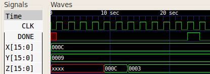
A simulation of the above code gave the following waveform which shows that gcd(12,9) = 3.