Propagation Delay
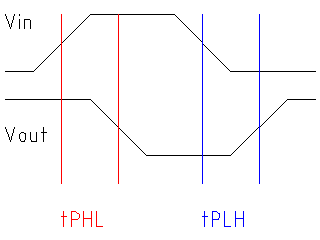
The propagation delay is the maximum amount of time it takes for a change in input signal give a change in output signal. With logic gates there are two possible transitions for the output signal: from high to low, and from low to high. The propagation delay for a gate to respond to a change in input and transition from high to low is named tPHL. Similarly the propagation delay for a transition from low to high is named tPLH. The propagation delay for the gate is taken as the maximum of tPHL and tPLH as this is the worst case delay. The picture below shows tPHL and tPLH on the input and output waveforms of a NOT gate. Here we've chosen a reference point at 50% of the high level voltage as the cross-over point from one logic level to the other.

Example
A data sheet for a 74HC00 quad 2-input NAND gate gives a propagation delay of 6.0ns.
References
Kleitz, W. Digital Microprocessor Fundamentals. 3rd Edition. Prentice Hall, 2000.
Mano, M. Morris, and Kime, Charles R. Logic and Computer Design Fundamentals. 2nd Edition. Prentice Hall, 2000.
74HC00 quad 2-input nand gate, NXP, 2011.