Counter
A counter is a register whose contents cycle through a predetermined sequence.
This cycle is driven by a clock.
The sequence does not have to be the usual binary code: 000, 001, 010, etc.
It may very well be an arbitrary sequence.
Example
The example given here is an arbitrary sequence 3-bit counter which cycles through four states.
This counter will be built around three edge triggered JK flip-flops.
The counter has three data output bits: Q0, Q1, and Q2.
Each output bit is connected to a flip-flop output and we will say that Q0 is the Q output of flip-flop 0.
There is a clock input, CLK which triggers the sequence changes.
There is also an active low reset input, RESETn which resets the flip-flops.
The state diagram is given below:

We can see that the states 011, 101, 110, and 111 are unused.
We will set them to transition to state 000.
The state table is shown below.
| Current State | Next State | ||||
|---|---|---|---|---|---|
Q2 |
Q1 |
Q0 |
Q2 |
Q1 |
Q0 |
0 | 0 | 0 |
0 | 0 | 1 |
0 | 0 | 1 |
0 | 1 | 0 |
0 | 1 | 0 |
1 | 0 | 0 |
0 | 1 | 1 |
0 | 0 | 0 |
1 | 0 | 0 |
0 | 0 | 0 |
1 | 0 | 1 |
0 | 0 | 0 |
1 | 1 | 0 |
0 | 0 | 0 |
1 | 1 | 1 |
0 | 0 | 0 |
The next step is determining the JK flip-flop inputs for creating the next state.
We will call the inputs of flip-flop 1 J1 and K1.
In the state table below X means "don't care".
| Current State | Next State | Flip-Flop Inputs | |||||||||
|---|---|---|---|---|---|---|---|---|---|---|---|
Q2 |
Q1 |
Q0 |
Q2 |
Q1 |
Q0 |
J0 |
K0 |
J1 |
K2 |
J2 |
K2 |
0 | 0 | 0 |
0 | 0 | 1 |
0 | X | 0 | X | 1 | X |
0 | 0 | 1 |
0 | 1 | 0 |
0 | X | 1 | X | X | 1 |
0 | 1 | 0 |
1 | 0 | 0 |
1 | X | X | 1 | 0 | X |
0 | 1 | 1 |
0 | 0 | 0 |
0 | X | X | 1 | X | 1 |
1 | 0 | 0 |
0 | 0 | 0 |
X | 1 | 0 | X | 0 | X |
1 | 0 | 1 |
0 | 0 | 0 |
X | 1 | 0 | X | X | 1 |
1 | 1 | 0 |
0 | 0 | 0 |
X | 1 | X | 1 | 0 | X |
1 | 1 | 1 |
0 | 0 | 0 |
X | 1 | X | 1 | X | 1 |
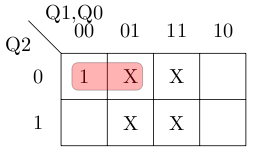
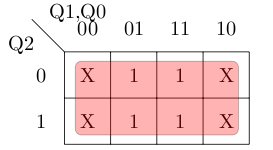
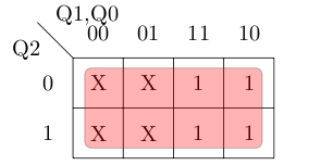
Now we can create the Karnaugh maps for the flip-flop inputs using the information in the table.
For J0 we get the map below giving us the equation not(Q2) and not(Q1).
For K0 we get the map below giving us the equation 1.
For J1 we get the map below giving us the equation Q0 and not(Q2).

For K1 we get the map below giving us the equation 1.
For J2 we get the map below giving us the equation not(Q0) and Q1.
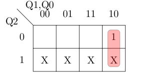
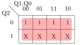
For K2 we get the map below giving us the equation 1.
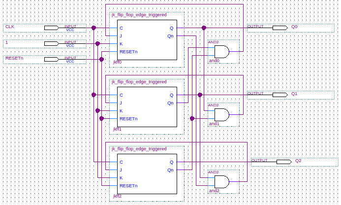
In schematic form we have the following:
Verilog
Below is a Verilog structural model for the counter. All code for the JK flip-flops is given as well.
module counter(Q2, Q1, Q0, CLK, RESETn);
   output Q2;
   output Q1;
   output Q0;
   input CLK;
   input RESETn;

   wire  Q2n;
   wire  Q1n;
   wire  Q0n;
   wire  J0;
   wire  J1;
   wire  J2;

   and(J2, Q1, Q0n);
   and(J1, Q0, Q2n);
   and(J0, Q1n, Q2n);

   jk_flip_flop_edge_triggered jkff0(Q0, Q0n, CLK, J0, 1'b1, RESETn);
   jk_flip_flop_edge_triggered jkff1(Q1, Q1n, CLK, J1, 1'b1, RESETn);
   jk_flip_flop_edge_triggered jkff2(Q2, Q2n, CLK, J2, 1'b1, RESETn);
endmodule // counter


module jk_flip_flop_edge_triggered(Q, Qn, C, J, K, RESETn);
   output Q;
   output Qn;
   input  C;
   input  J;
   input  K;
   input  RESETn;

   wire   Kn;   // The complement of the K input.
   wire   D;
   wire   D1;   // Data input to the D latch.
   wire   Cn;   // Control input to the D latch.
   wire   Cnn;  // Control input to the SR latch.
   wire   DQ;   // Output from the D latch, inputs to the gated SR latch (S).
   wire   DQn;  // Output from the D latch, inputs to the gated SR latch (R).

   assign D1 = !RESETn ? 0 : D;  // Upon reset force D1 = 0

   not(Kn, K);
   and(J1, J, Qn);
   and(K1, Kn, Q);
   or(D, J1, K1);
   not(Cn, C);
   not(Cnn, Cn);
   d_latch dl(DQ, DQn, Cn, D1);
   sr_latch_gated sr(Q, Qn, Cnn, DQ, DQn);
endmodule // jk_flip_flop_edge_triggered

module d_latch(Q, Qn, G, D);
   output Q;
   output Qn;
   input  G;
   input  D;

   wire   Dn;
   wire   D1;
   wire   Dn1;

   not(Dn, D);
   and(D1, G, D);
   and(Dn1, G, Dn);
   nor(Qn, D1, Q);
   nor(Q, Dn1, Qn);
endmodule // d_latch

module sr_latch_gated(Q, Qn, G, S, R);
   output Q;
   output Qn;
   input  G;
   input  S;
   input  R;

   wire   S1;
   wire   R1;

   and(S1, G, S);
   and(R1, G, R);
   nor(Qn, S1, Q);
   nor(Q, R1, Qn);
endmodule // sr_latch_gated
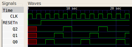
Below you can see the waveforms produced when the counter was reset and the the clock left to run.
References
Mano, M. Morris, and Kime, Charles R. Logic and Computer Design Fundamentals. 2nd Edition. Prentice Hall, 2000.