Sequential Logic Design Example (Traffic Lights)
The following is an example of a sequential logic design.
Problem Description
Imagine we wanted to design a traffic light system with a pedestrian crossing function.
Pedestrians could push a button to request that the traffic be signalled to stop to provide them with a safe crossing.
Such a system would have three lights for the vehicles on the road: red, yellow, and green.
Let's call these signals R, Y, and G.
For the pedestrians we would have a light to signal that the traffic has been stopped and it is safe to cross.
Let's call this signal M ('M' for man — the signal is usually a green walking man).
We'll also need an input button for pedestrians to push when they want to cross the road. Let's call this B.
The pedestrian pushes the button and if the traffic light system is signalling G
then the signalling sequence is as follows:
- Signal
Y. This prepares the traffic for a stop. - Signal
R. This stops the traffic. - Signal
MandR. This informs the pedestrian that it is safe to cross. - Signal
R. This keeps the traffic at a standstill and lets pedestrians finish their crossing. - Signal
G. This permits the traffic to start moving again.
Button presses for the first three steps will be ignored — a crossing has already been requested. A button push during the last two steps will be remembered and trigger a new sequence when the current one is finished.
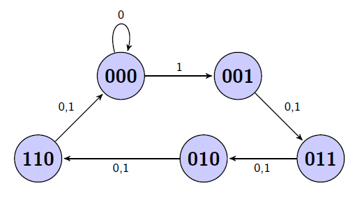
State Diagram
Each step in the sequence will map to one state. We'll number them using a binary code:
000- signalG.001- signalY.011- signalR.010- signalMandR.110- signalR.
From this we can create the state diagram below.
The input used in the diagram is B.
The outputs are not shown as this is a Moore model and showing these outputs in the table given below suffices.
State Table
Using the information from the state diagram above and the outputs generated in each state, we can build a
state table.
With three state bits and one input, we have 16 (23+1=16) different possibilities.
Many of these should never occur so we can either ignore them or force them into a fail-safe configuration.
In this case we'll make the unused states (100, 101, and 110) transition to
state 001 (yellow light) regardless of input B.
| State | Input | State | Output | |||||||
|---|---|---|---|---|---|---|---|---|---|---|
| Current | B |
Next | M |
R |
Y |
G |
||||
0 | 0 | 0 |
0 |
0 | 0 | 0 |
0 | 0 | 0 | 1 |
0 | 0 | 0 |
1 |
0 | 0 | 1 |
0 | 0 | 0 | 1 |
0 | 0 | 1 |
0 |
0 | 1 | 1 |
0 | 0 | 1 | 0 |
0 | 0 | 1 |
1 |
0 | 1 | 1 |
0 | 0 | 1 | 0 |
0 | 1 | 0 |
0 |
1 | 1 | 0 |
1 | 1 | 0 | 0 |
0 | 1 | 0 |
1 |
1 | 1 | 0 |
1 | 1 | 0 | 0 |
0 | 1 | 1 |
0 |
0 | 1 | 0 |
0 | 1 | 0 | 0 |
0 | 1 | 1 |
1 |
0 | 1 | 0 |
0 | 1 | 0 | 0 |
1 | 0 | 0 |
0 |
0 | 0 | 1 |
0 | 0 | 1 | 0 |
1 | 0 | 0 |
1 |
0 | 0 | 1 |
0 | 0 | 1 | 0 |
1 | 0 | 1 |
0 |
0 | 0 | 1 |
0 | 0 | 1 | 0 |
1 | 0 | 1 |
1 |
0 | 0 | 1 |
0 | 0 | 1 | 0 |
1 | 1 | 0 |
0 |
0 | 0 | 0 |
0 | 1 | 0 | 0 |
1 | 1 | 0 |
1 |
0 | 0 | 0 |
0 | 1 | 0 | 0 |
1 | 1 | 1 |
0 |
0 | 0 | 1 |
0 | 0 | 1 | 0 |
1 | 1 | 1 |
1 |
0 | 0 | 1 |
0 | 0 | 1 | 0 |
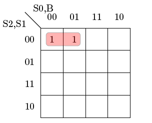
Logic Design
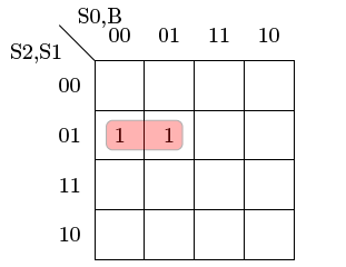
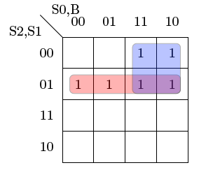
From the state table we can create Karnaugh maps and from these generate the logic equations for the outputs
and the next state.
In the maps, the column S0 is the least significant state bit, and B is B.
In the rows, S2 is the most significant state bit.
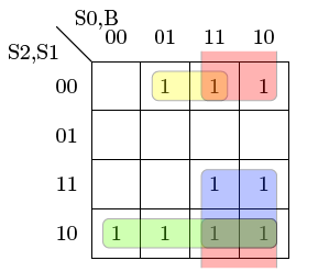
From the Karnaugh map for the most significant next state bit, which is shown below, we get an equation of not(S0) and S1 and not(S2).
From the Karnaugh map for the middle next state bit, which is shown below, we get an equation of (S1 and not(S2)) or (S0 and not(S2)).
From the Karnaugh map for the least significant next state bit, which is shown below, we get an equation of (not(S1) and S2) or (S0 and S2) or (S0 and not(S1)) or (B and not(S1) and not(S2)).
From the Karnaugh map for the M signal output, shown below, we get an equation of not(S0) and S1 and not(S2).
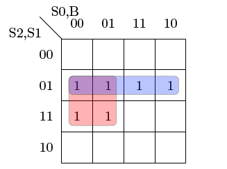
From the Karnaugh map for the R signal output, shown below, we get an equation of (not(S0) and S1) or (S1 and not(S2)).
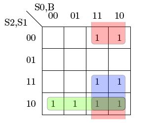
From the Karnaugh map for the Y signal output, shown below, we get an equation of (not(S1) and S2) or (S0 and S2) or (S0 and not(S1)).
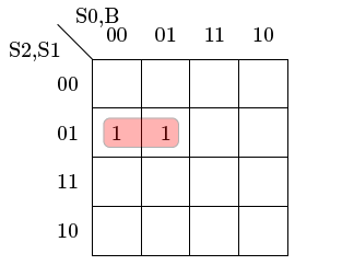
From the Karnaugh map for the G signal output, shown below, we get an equation of not(S0) and not(S1) and not(S2).
Implementation
The full Verilog code for the implementation of the design is shown below.
The only change between this implementation and the original design is the inclusion of an active low
reset input (RESETn).
A reset will force the circuit into state 000.
We also use a SR latch to remember button presses.
We reset this latch when M is signalled. This will give us the button functionality we require.
module traffic_lights_example(M, R, Y, G, Button, CLK, RESETn);
   output M;          // Green Man output light.
   output R;          // Red traffic signal light.
   output Y;          // Yellow (Amber) traffic signal light.
   output G;          // Green traffic signal light.
   input  Button;     // Pedestrian push button.
   input  CLK;        // System clock.
   input  RESETn;     // System reset.

   wire   S0;          // Current state least significant bit.
   wire   S1;
   wire   S2;          // Current state most significant bit.
   wire   S0n;         // Current state least significant bit.
   wire   S1n;
   wire   S2n;         // Current state most significant bit.
   wire   Next0;       // Next state least significant bit.
   wire   Next1;
   wire   Next2;       // Next state most significant bit.
   wire   ButtonReset; // Used to reset the push button SR flip-flop.
   wire   B;           // Output from the button state SR latch.
   wire   Bn;          // The complement of B.
   wire   w1, w2, w3, w4, w5, w6, w7, w8, w9, w10, w11, w12, w13; // Linking wires.

   d_flip_flop_edge_triggered state0(S0, S0n, CLK, Next0);
   d_flip_flop_edge_triggered state1(S1, S1n, CLK, Next1);
   d_flip_flop_edge_triggered state2(S2, S2n, CLK, Next2);
   sr_latch_ungated button_state(B, Bn, Button, ButtonReset);

   // ButtonReset = !RESETn | M;
   not(RESET, RESETn);
   or(ButtonReset, RESET, M);

   // Next0 = !RESETn ? 1'b0 : (S1n & S2) | (S0 & S2) | (S0 & S1n) | (B & S1n & S2n);
   and(w1, S1n, S2);
   and(w2, S0, S2);
   and(w3, S0, S1n);
   and(w4, B, S1n, S2n);
   or(w5, w1, w2, w3, w4);
   and(Next0, RESETn, w5);

   // Next1 = !RESETn ? 1'b0 : (S0 & S2n) | (S1 & S2n);
   and(w6, S0, S2n);
   and(w7, S1, S2n);
   or(w8, w6,w7);
   and(Next1, RESETn, w8);

   // Next2 = !RESETn ? 1'b0 : S0n & S1 & S2n;
   and(Next2, RESETn, S0n, S1, S2n);

   // M = not(S0) and S1 and not(S2)
   and(M, S0n, S1, S2n);

   // R = (not(S0) and S1) or (S1 and not(S2))
   and(w9, S0n, S1);
   and(w10, S1, S2n);
   or(R, w9, w10);

   // Y = (not(S1) and S2) or (S0 and S2) or (S0 and not(S1))
   and(w11, S1n, S2);
   and(w12, S0, S2);
   and(w13, S0, S1n);
   or(Y, w11, w12, w13);

   // G = not(S0) and not(S1) and not(S2)
   and(G, S0n, S1n, S2n);
endmodule // traffic_lights_example

module d_flip_flop_edge_triggered(Q, Qn, C, D);
   output Q;
   output Qn;
   input  C;
   input  D;

   wire   Cn;   // Control input to the D latch.
   wire   Cnn;  // Control input to the SR latch.
   wire   DQ;   // Output from the D latch, inputs to the gated SR latch.
   wire   DQn;  // Output from the D latch, inputs to the gated SR latch.

   not(Cn, C);
   not(Cnn, Cn);
   d_latch dl(DQ, DQn, Cn, D);
   sr_latch_gated sr(Q, Qn, Cnn, DQ, DQn);
endmodule // d_flip_flop_edge_triggered

module d_latch(Q, Qn, G, D);
   output Q;
   output Qn;
   input  G;
   input  D;

   wire   Dn;
   wire   D1;
   wire   Dn1;

   not(Dn, D);
   and(D1, G, D);
   and(Dn1, G, Dn);
   nor(Qn, D1, Q);
   nor(Q, Dn1, Qn);
endmodule // d_latch

module sr_latch_gated(Q, Qn, G, S, R);
   output Q;
   output Qn;
   input  G;
   input  S;
   input  R;

   wire   S1;
   wire   R1;

   and(S1, G, S);
   and(R1, G, R);
   nor(Qn, S1, Q);
   nor(Q, R1, Qn);
endmodule // sr_latch_gated

module sr_latch_ungated(Q, Qn, S, R);
   output Q;
   output Qn;
   input  S;
   input  R;

   nor(Qn, S, Q);
   nor(Q, R, Qn);
endmodule // sr_latch_ungated
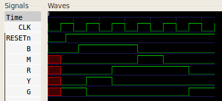
The simulation gave the following results with a test button push:
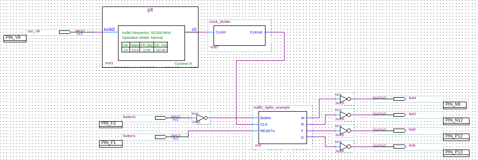
The design was used to program the FPGA found on the Altera Cyclone III Starter Kit.
Two push buttons on the board were used for the reset input and the pedestrian button.
As the buttons gave a 0 input when pushed, the pedestrian button had to be inverted.
The four board LEDs were used for M, R, Y, and G.
The LEDs were illuminated when 0 was output to the appropriate pins.
Because of this, the output signals were inverted.
The board clock of 50Mhz was run through a clock divider to give a state transition frequency that was easier
for the human eye to recognise.
The top-level schematic is shown below: